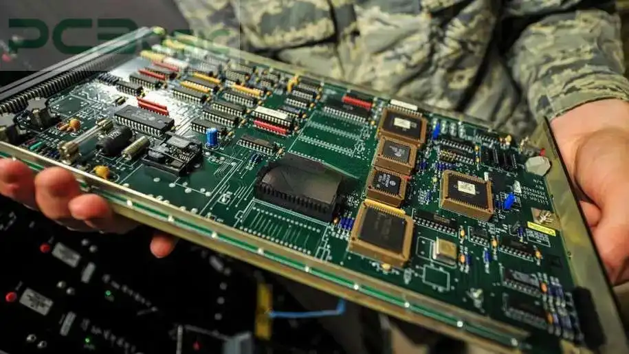
Sequential Build-Up PCB
Sequential Build-Up PCB technology represents a cornerstone in advanced printed circuit board manufacturing, enabling the creation of high-density interconnect (HDI) boards through a layered construction process. In this approach, dielectric and conductive layers are added sequentially to a core substrate, often incorporating microvias and buried vias to achieve finer pitches and greater functionality in compact spaces. This method is particularly valuable for engineers and designers working on modern electronics, where space constraints and performance demands are ever-increasing, such as in smartphones, medical devices, automotive systems, and aerospace applications. For those searching for Sequential Build-Up PCB, understanding its implementation can directly impact design efficiency and product reliability. Key advantages include enhanced signal integrity due to reduced layer counts in some configurations, improved thermal management through strategic material selection, and cost-effective scalability for high-volume production. Best practices involve careful layer stacking to minimize warpage, selecting appropriate dielectric materials like high-Tg FR-4 or polyimide for thermal stability, and employing laser drilling for precise microvia formation. Designers should also prioritize simulation tools to model impedance and crosstalk early in the process, ensuring compliance with standards like IPC-2226 for HDI boards. By delving into the articles tagged under Sequential Build-Up PCB, readers can gain practical guidance on optimizing build-up sequences, troubleshooting common fabrication issues, and integrating this technology with emerging trends like 5G and IoT. These resources offer step-by-step insights into real-world case studies, helping professionals refine their approaches and achieve superior board performance in demanding environments.
Technical Articles
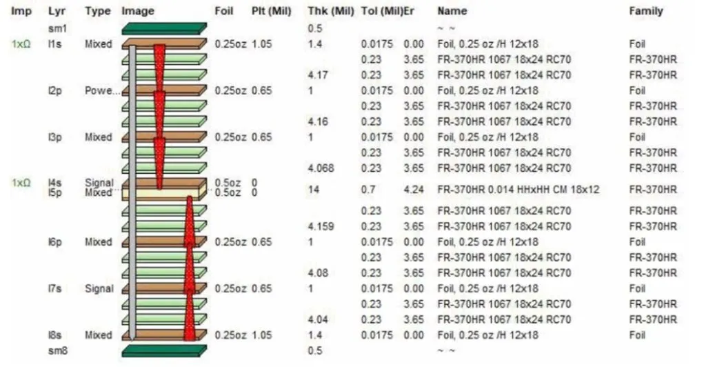
Blind and Buried Vias in Sequential Build Up PCBs: Design and Fabrication Techniques
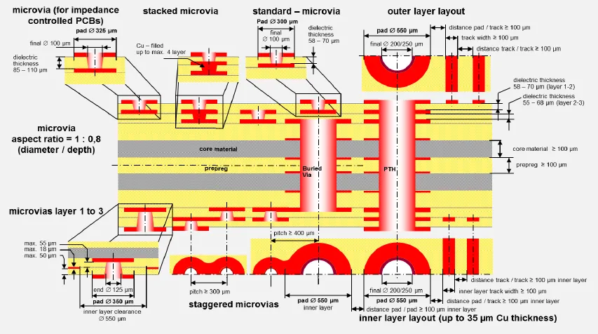
Demystifying Sequential Build Up PCBs: A Beginner's Guide to HDI Technology
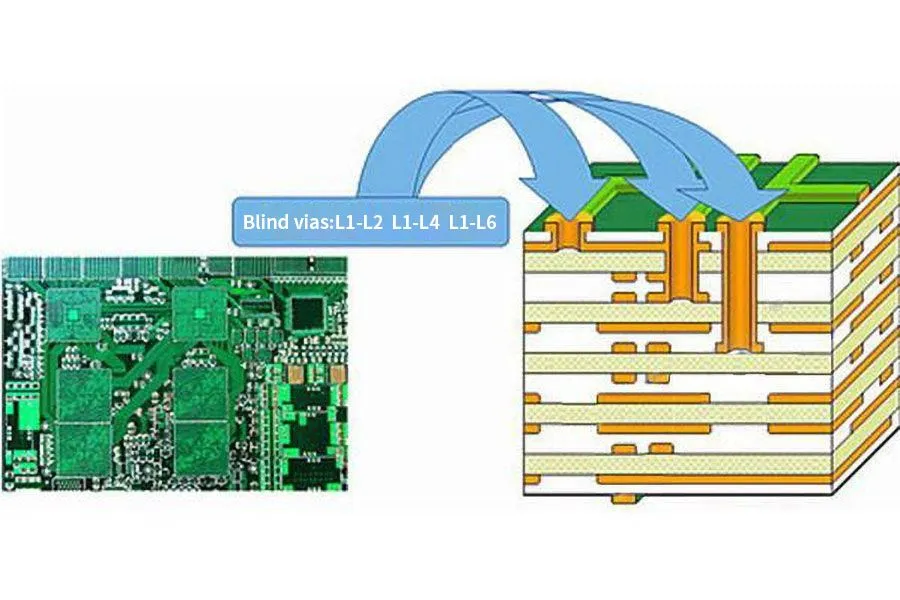
Sequential Build Up PCBs for Automotive Electronics: Meeting Demanding Performance and Reliability Requirements
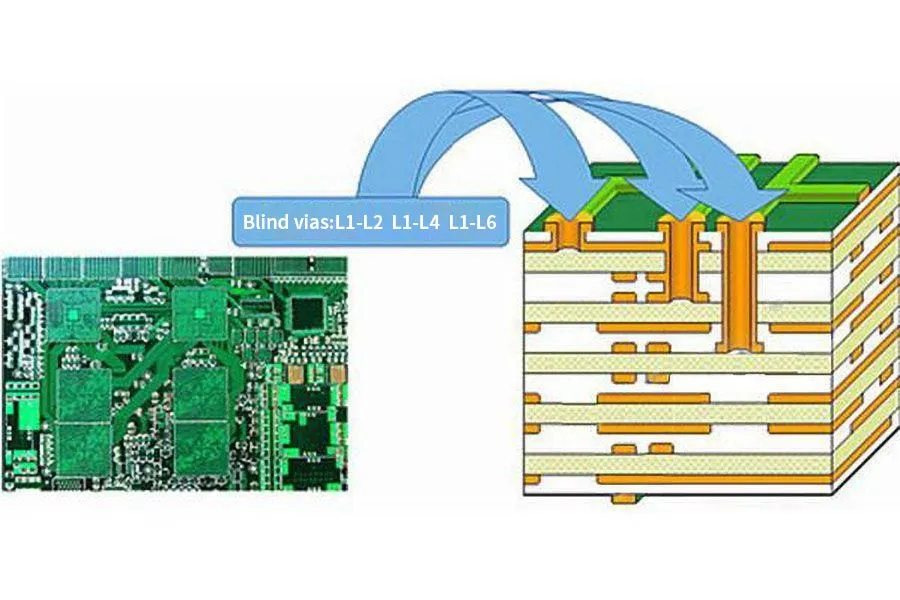
Cost Effective Sequential Build Up PCB Design: Strategies for Reducing Manufacturing Expenses
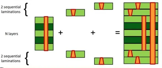
Troubleshooting Challenges in Sequential Build Up PCB Manufacturing: A Practical Guide
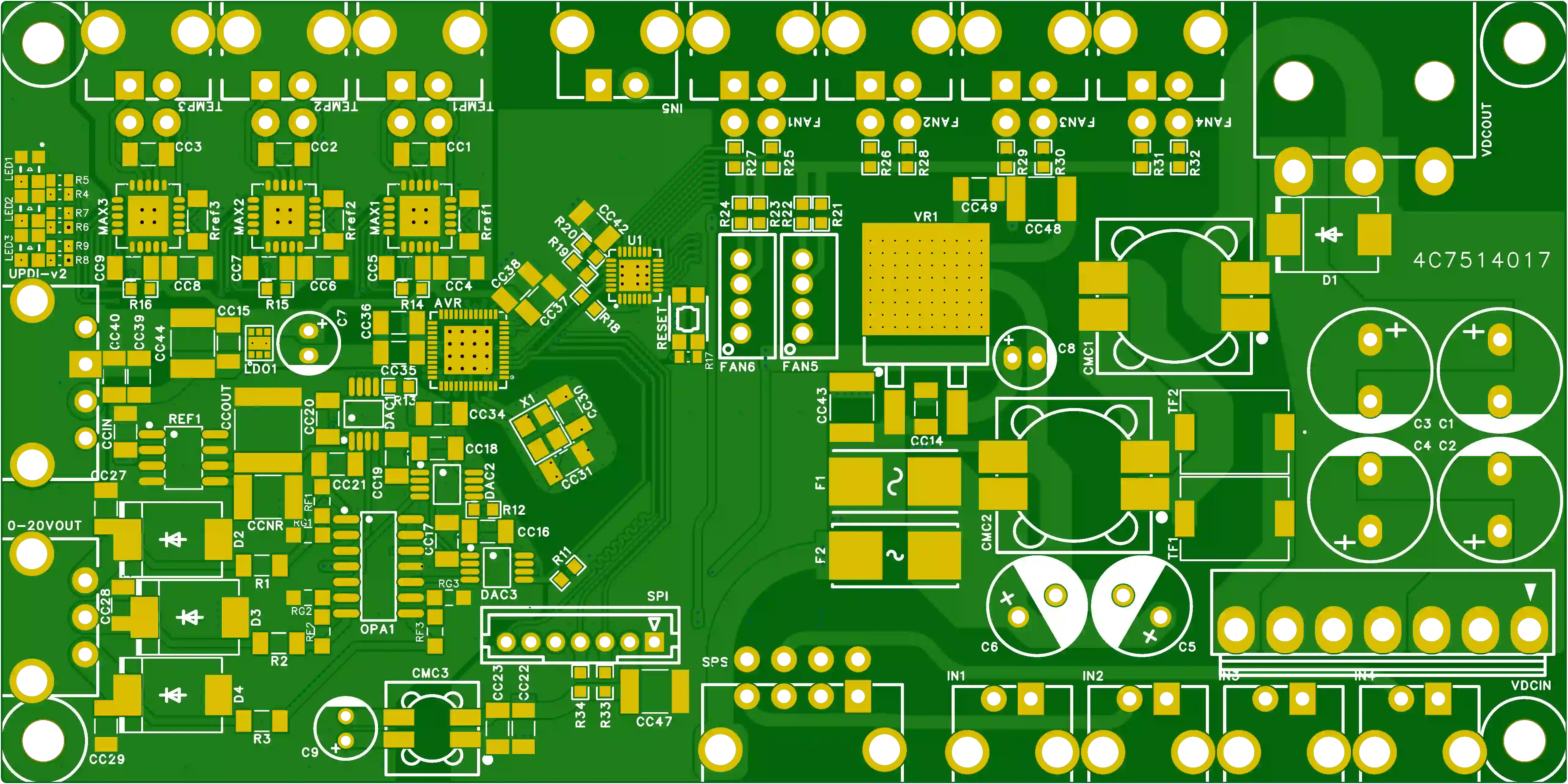
How Conflicting Via Data and Soldermask Definitions Triggered CAM Review in a 4-Layer HDI PCB
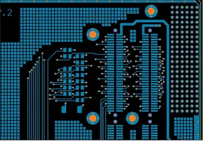
Why HDI PCB Manufacturers Add Dummy Copper
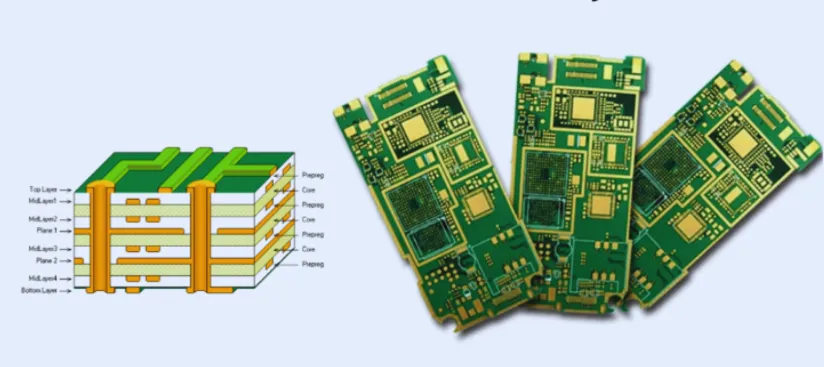
Crafting Multi-Layer PCBs at Home: A Hobbyist’s Guide to Advanced Board Fabrication
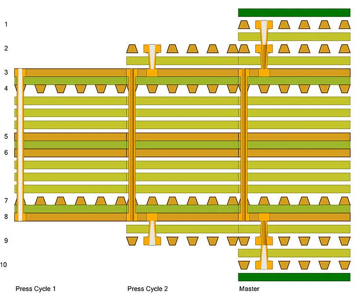
Troubleshooting Sequential Lamination: Avoiding Delamination, Resin Cracks, and Voids
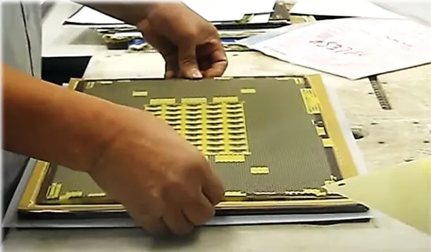
Sequential Lamination for High-Speed Designs: Minimizing Signal Loss and Maximizing Performance
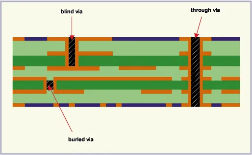
Sequential Lamination in HDI PCBs: The Definitive Guide to Blind and Buried Vias
Get in Touch
Send Message
- Products & Service
- Company
- About AIVON
- Contact
- News
- Blog
- Certification
-


- Payment
-


2026 AIVON.COM All Rights Reserved