










Inside the Reflow Oven: What Really Goes Wrong in PCBA Manufacturing
Key Moment
What This Video Covers
This video takes engineers inside a multi-zone reflow oven—the thermal process every SMT assembly must survive. Heating solder paste until it melts sounds simple. In production, even a millisecond wetting mismatch or an unbalanced copper stack-up can open a joint, stand a 0402 resistor on end, or crack a ceramic capacitor after the profile looks "in spec."
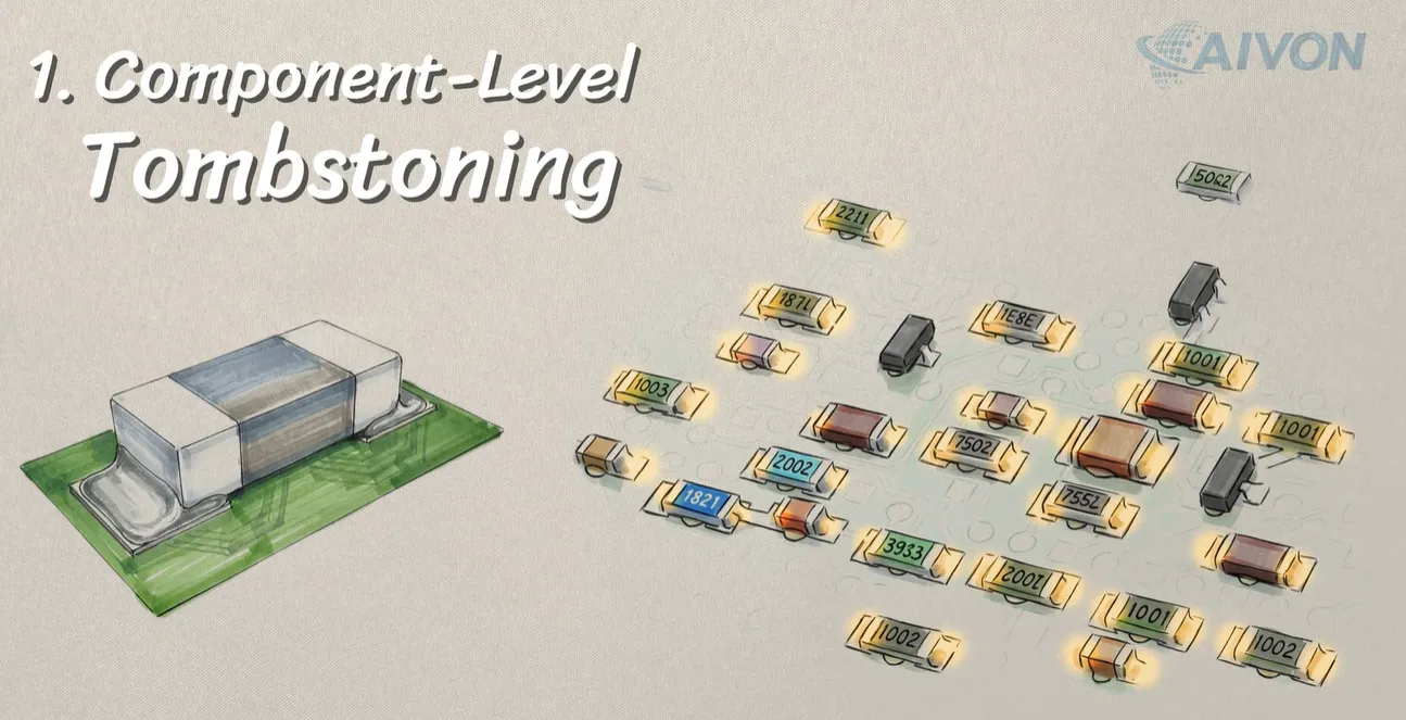
The walkthrough starts at the component level: tombstoning, where liquid solder on one pad pulls a chip passive upright before the opposite termination reaches liquidus.
It then moves to board-level risk—CTE mismatch between FR-4 resin, copper foil, and prepreg that bows the laminate and loads fragile parts. The later sequences cover defects that AOI cannot always see: BGA voiding and head-in-pillow, where package warpage separates balls from printed paste.
Those mechanisms matter on turnkey PCB assembly for automotive controllers, medical instruments, and industrial I/O, especially on HDI PCB and multilayer FR4 PCB designs with mixed thermal mass. Use the footage to brief DFM reviews, then request a PCB assembly quote with profile and stack-up notes attached.
Key Highlights
- Tombstoning is a wetting-time failure: if one pad of a small passive reaches liquidus milliseconds before the other, molten-solder surface tension stands the part vertical and opens the circuit.
- A "good" thermal profile does not cancel board warpage. Unbalanced copper, prepreg, and resin expansion still flex the laminate and can crack MLCC bodies after reflow.
- BGA voids and head-in-pillow hide under the package. Package warpage plus paste/flux behavior can leave balls sitting on uncollapsed solder instead of forming a continuous joint.
How Tombstoning Forms When Pad Wetting Is Unbalanced
Every SMD assembly travels through the reflow oven so hundreds of terminations can wet, collapse, and freeze into metallurgical joints. In the peak zone, solder paste stops being a paste and becomes a liquid alloy. For a two-terminal chip resistor or capacitor, both ends must melt in the same narrow window. When they do not, the first liquid fillet exerts an immediate pulling force.
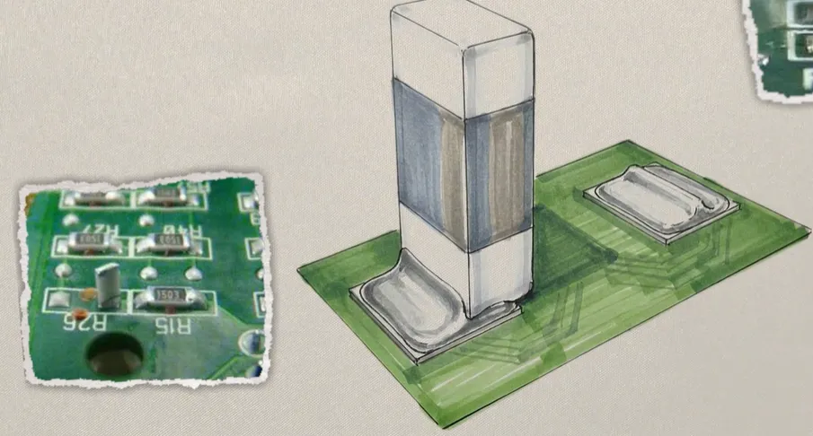
That force is surface tension, not gravity. The wetted terminal is yanked toward the pad while the cold side still sits on unmelted paste. With no opposing fillet, the body rotates until it stands on one end—the classic tombstone. A micro-second mismatch in heat absorption is enough. The finished board then carries an open circuit that electrical test may catch, but only after the panel has already consumed paste, placement time, and oven capacity.
Factory data usually traces the mismatch to thermal mass, not a "bad oven" in isolation. A pad tied into a wide copper pour or a via farm heats and melts later than a pad sitting on a thin trace. Unequal stencil apertures dump more paste on one side and increase the wetting force once that side liquefies. HASL thickness variation, part tombstone-prone packages (0201/0402), and an aggressive preheat ramp all widen the same window.
DFM that actually reduces tombstones is geometric and thermal at the same time: matched pad sizes per IPC-7351, thermal reliefs on heavy copper, vias kept off the pad, balanced paste volume through a controlled SMT stencil, and a preheat ramp held near 1–2 °C/s so both terminations approach liquidus together. Orientation relative to conveyor airflow is a secondary but cheap control—align the long axis of chip parts with belt travel when the layout allows.
Board Warpage, CTE Mismatch, and Hidden Mechanical Stress
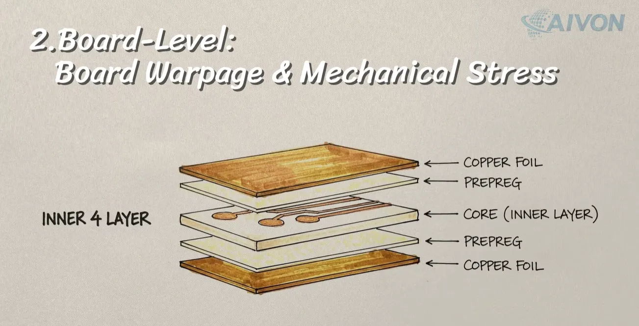
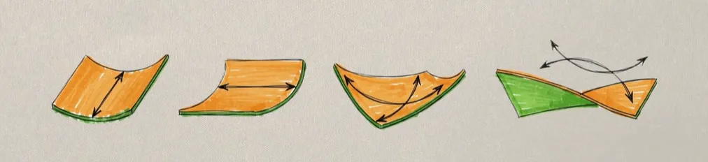
Tombstoning moves one component. Warpage moves the whole board. A rigid PCB is not a single material. It is a laminate of glass-reinforced resin, copper foil, and prepreg. Each layer expands at a different rate as the panel climbs through preheat, soak, and peak. When copper is dense on one side and sparse on the other, the stack behaves like a bimetallic strip. The resin-rich face wants to grow; the copper-rich face restrains it. The panel bows or twists.
That shape change is not cosmetic. A bowed board changes standoff height under large packages, lifts corners of QFNs, and puts tensile or shear load into solder joints that have not yet frozen. For ceramic capacitors, the risk is internal. The brittle dielectric does not stretch with the FR-4. Excessive flex during or immediately after peak can nucleate flex cracks that later fail as intermittent opens in the field—especially on automotive PCB and industrial control PCB products that see vibration after assembly.
Warpage is worse on thin cores, large panels, heavy copper on one outer layer, and unbalanced 4 layer PCB or 6 layer PCB stack-ups. A high TG PCB raises the temperature at which the resin softens, which helps, but it does not cancel an asymmetric copper map. Slow conveyor speed that parks the board too long near peak also overheats the resin and increases sag.
Process-side controls are mechanical as much as thermal: center-board support or a reflow pallet on long/thin panels, balanced copper pours and dummy copper on sparse layers, matched prepreg and core construction, and a cooling slope that does not shock the laminate. Specify bow and twist limits on the fabrication drawing (commonly ≤0.75% for Class 3) and verify them after reflow, not only at incoming bare-board inspection.
Hidden Package Defects: BGA Voids and Head-in-Pillow
As designs move into high-density packaging, the most expensive reflow defects leave the surface. A BGA hides hundreds of joints under the body. AOI sees the package outline; it does not see whether every ball collapsed into a continuous fillet.
Voiding forms when flux volatiles or trapped air cannot escape before the joint freezes. Large ground pads, microvia-in-pad without fill/cap, wet paste printed too thick, and a soak that is too short or too cool all raise void area. A few percent voiding is common. Excessive voids cut thermal and electrical cross-section and become crack starters under power cycling on power supply PCB and compute modules.
Head-in-pillow is a different geometry. The BGA substrate itself warps as it heats. Balls lift off the printed paste, the paste reflows into a rounded "pillow," and the ball sits on that pillow without merging. After cool-down the joint can look almost circular on X-ray yet have no reliable metallurgical bond. Dynamic warpage of the package, an oxidized ball surface, depleted flux, and a peak that is only barely above liquidus are the usual combination.
These defects are why a reflow conversation cannot stop at "peak temperature was 245 °C." Package warpage curves, paste alloy and flux activity, stencil design for BGA pads, and nitrogen vs. air atmosphere all sit inside the same process window as the chip-passive tombstone problem. X-ray and, where justified, cross-section are the inspection pair—not a substitute for stack-up and paste-print control.
DFM and Process Controls That Reduce Reflow Failures
The useful question for an OEM engineer is not "did the oven hit the datasheet curve?" It is "did both ends of every small passive, and every BGA ball, experience the same thermal and mechanical history?" That is a layout, stack-up, stencil, and profile problem at once.
On the design side, equalize copper connected to opposite pads of chip parts, keep thermal vias a safe distance from those pads, and avoid mixing a tiny 0201 next to a large connector that shadows airflow. On multilayer boards, mirror copper density through the stack and call out high-Tg material when peak temperature and board thickness would otherwise soften the resin. On the print side, keep stencil thickness and aperture reduction consistent so paste volume does not become another wetting imbalance.
On the oven side, profile the real product—not a coupon in the panel center only. Place thermocouples on a high-mass ground region and on a low-mass 0402 site. Hold preheat ramps conservative, give flux a real soak, keep time above liquidus inside the paste window, and support the panel so gravity plus CTE does not add a new stress. Then inspect with the method that can actually see the defect: AOI for tombstones and skew, X-ray for BGA voids and head-in-pillow.
| Defect | Primary mechanism in the oven | Typical design / print trigger | Factory control that actually moves yield |
|---|---|---|---|
| Tombstoning | One pad reaches liquidus first; surface tension lifts the chip | Unequal pads, copper imbalance, 0201/0402, uneven paste | Matched pads, thermal reliefs, 1–2 °C/s preheat, balanced stencil apertures |
| Board warpage / MLCC crack | CTE mismatch + resin softening + sag | Unbalanced stack-up, thin core, heavy copper on one side | Balanced copper, high-Tg laminate, center support / pallet, bow/twist spec after reflow |
| BGA voiding | Gas trapped as joint freezes | Via-in-pad, thick paste, short soak | Filled/capped vias, soak 60–120 s, nitrogen if specified, X-ray criteria |
| Head-in-pillow | Package warpage separates ball from paste | Dynamic package warp, weak flux, marginal peak | Package-aware profile, adequate TAL, coplanarity control, X-ray / dye-and-pry on quals |
| Profile / design parameter | Practical production window | Why it matters in the reflow oven |
|---|---|---|
| Preheat ramp | 1–2 °C/s (stay below ~3 °C/s) | Limits ΔT across tiny passives and reduces tombstoning |
| Soak | 150–180 °C, typically 60–120 s for SAC | Activates flux and evens temperature before peak |
| Peak / TAL (SAC305) | ~235–245 °C; time above liquidus ~45–90 s | Completes wetting without overheating the laminate or growing excessive IMC |
| Cooling | ~3–6 °C/s, controlled | Limits IMC growth and thermal shock that cracks ceramics |
| Bow / twist after reflow | Often ≤0.75% for Class 3 | Warped boards change standoff and load solder joints |
| Small-passive risk | Highest on 0201 / 0402 | Low mass cannot resist unbalanced wetting force |
If the design cannot change—fixed 0201 population, thick copper power plane, large BGA—say so on the PCB assembly quote package. A manufacturer that profiles the real stack-up and prints a matched stencil will still have a process window. One that only copies a generic "lead-free curve" will not.
FAQ
Q1: Does a correct reflow profile guarantee no tombstoning on 0402 parts?
A1: No. Profile is necessary, not sufficient. If one pad is tied to a copper pour and the other is not, or if stencil apertures deposit unequal paste, one termination still reaches liquidus first. Fix pad symmetry, copper connection, and print volume first; then slow the preheat ramp so both sides arrive together.
Q2: Can board warpage occur even when peak temperature is within the paste datasheet?
A2: Yes. Warpage is a stack-up and support problem as much as a peak-temperature problem. Unbalanced copper, thin cores, and unsupported long panels sag when the resin softens near peak. The profile can look acceptable on a center thermocouple while the panel is already bowed.
Q3: When should we require X-ray instead of AOI after reflow?
A3: Whenever joints are hidden: BGAs, LGAs, QFNs with center pads, and via-in-pad structures. AOI will catch tombstones, skew, and missing chips. It will not quantify BGA void area or confirm that a ball merged with the printed deposit instead of sitting in a head-in-pillow geometry.
Q4: Is high-Tg FR-4 enough to stop reflow warpage on a multilayer board?
A4: High-Tg material raises the temperature at which the resin softens and is the right call for many lead-free, multilayer, and automotive builds. It does not cancel an asymmetric copper map. Balance the stack, add dummy copper where needed, and use center-board support or a pallet on large, thin panels.
Q5: Which is more expensive to ignore in production—tombstoning or BGA head-in-pillow?
A5: Tombstoning is cheaper to detect and rework; it is visible and usually fails ICT or flying probe. Head-in-pillow can escape AOI, pass a weak functional test, and fail after thermal cycling in the field. For BGA-heavy designs, budget X-ray sampling and a package-aware profile before volume ramps.
This, is a reflow oven.Every SMD assembly passes through here, where hundreds of components are heated and soldered onto the PCB.
It sounds simple: heat it up, melt the solder, and let it cool.
But inside this oven, things are far more complicated.The temperature changes across multiple stages, and even a small deviation in the thermal profile can affect how those tiny solder joints form.
But we're not going to dive into complicated temperature curves today.Instead, let's take a look at what happens when things go wrong inside the reflow oven.
1. Component-Level: Tombstoning (Surface Tension Unbalanced)
One of the most visible failures is tombstoning.As the board enters the peak reflow zone, solder paste transitions into a liquid alloy. For small passive components—like chip resistors or capacitors—both ends are supposed to melt simultaneously.
However, if one pad reaches the melting point just milliseconds before the other—due to uneven thermal mass or trace layout—the molten solder on that side instantly wets the terminal. The liquid surface tension creates a powerful pulling force. With no counter-tension on the cold side, the component is yanked upward, standing completely vertical on one end like a tombstone.
However, if one pad heats up and melts solder before the other, surface tension pulls the component toward the molten side—lifting it upright like a tombstone
A micro-second mismatch in heat absorption transforms a functional component into an open circuit.
2. Board-Level: Board Warpage & Mechanical Stress
But sometimes, it's not just the component that moves. The entire board can deform.
A PCB combines fiberglass-reinforced resin, copper, and prepreg, and these materials expand differently as temperature changes.
During reflow, this mismatch in thermal expansion can create mechanical stress and contribute to board warpage—especially when the stackup or copper distribution is unbalanced.
That warpage can put additional mechanical stress on components and solder joints. For fragile ceramic capacitors, excessive board flexing can even lead to internal cracking.
So even when the reflow profile looks correct, board-level deformation can still become a hidden source of assembly defects.





