Many beginners finish a clean schematic in KiCad only to struggle once they open the PCB Editor. Components end up scattered, traces cross unnecessarily, design rules are ignored until the last minute, and the board that reaches the manufacturer needs expensive changes. The layout stage is where electrical intent becomes a physical, manufacturable product—and where most costly mistakes are made.
This guide walks through the complete PCB layout process in KiCad for beginners. You will learn how to prepare the board correctly, place components with real engineering considerations, route reliably, run proper checks, and design with manufacturing constraints in mind so the finished board can actually be fabricated and assembled without surprises.
PCB Layout Preparation
Before placing a single component, set up the board environment. Skipping this step forces repeated fixes later and often leads to design-rule violations that only appear during manufacturing review.
Board Settings
Open the Board Setup dialog and define the board outline (Edge.Cuts layer). Set the correct page size, grid, and units (millimeters are standard for most fabricators). Add mounting holes and keep-out areas early if the mechanical design is already fixed.
Layer Setup
Choose the layer stack that matches your intended manufacturer. For most beginner and intermediate projects a 2-layer or 4-layer stack is sufficient. Name the layers clearly and enable only the layers you will actually use. Add a note about the intended stack-up (copper weight, dielectric thickness, surface finish) so it travels with the design files.
Design Rules
Load or create design rules that reflect the fabricator's capabilities, not KiCad's defaults. Set minimum track width, clearance, via diameter, annular ring, and hole size according to the manufacturer's process limits. Create net classes for power, ground, and critical signals so the router and DRC enforce the correct values automatically.
Manufacturing perspective: rules that are tighter than the fab can produce cause yield loss or extra charges. Defining realistic rules at the start prevents the common situation where a finished layout must be reworked after the manufacturer's DFM review.

Component Placement Best Practices
Placement quality determines how easy routing will be and how well the finished board performs. Poor placement creates long traces, extra vias, thermal hotspots, and signal-integrity problems that are difficult to fix later.
Place connectors, crystals, power regulators, and high-speed ICs first. Group functional blocks together and keep analog and digital sections separated when possible. Orient similar components in the same direction to simplify assembly and inspection.
Signal Integrity Considerations
Keep high-speed and sensitive traces short. Place decoupling capacitors as close as possible to the power pins they serve. Avoid placing noisy digital components next to analog sections or crystal oscillators.
Thermal Considerations
Identify components that dissipate significant heat (regulators, power MOSFETs, LED drivers). Provide copper area or thermal vias under their pads and leave space for airflow or heatsinks if needed. Do not bury heat-generating parts under other components or near temperature-sensitive devices.
Manufacturing perspective: placement that ignores thermal or mechanical constraints forces the assembler to deal with tombstoning risk, difficult rework, or mechanical interference. Good placement reduces both fabrication and assembly risk.

Routing in KiCad
Once placement is stable, begin routing. Start with power and ground, then critical signals, and finish with general nets.
Trace Width
Assign track widths according to the net classes defined earlier. Power traces must be wide enough for the expected current; signal traces can be narrower. Use the interactive router so it respects the rules automatically.
Via Usage
Use vias only when necessary. Each via adds inductance, costs an extra drill operation, and slightly reduces reliability. When vias are required, choose sizes that meet the manufacturer's minimum annular ring and hole-size rules. Avoid via-in-pad unless the design and fabricator specifically support it.
Differential Pairs
For USB, Ethernet, HDMI, or other differential signals, use KiCad's differential pair routing tools. Set the correct gap and length matching rules. Keep the pair tightly coupled and avoid unnecessary layer changes.
Manufacturing perspective: tracks that violate minimum width or clearance, or vias that fall below the fab's annular-ring limit, are common reasons for DFM rejection. Routing within the manufacturer's process window keeps cost and lead time predictable.

Running PCB Checks Before Manufacturing
Never generate manufacturing files until the board has passed a full Design Rule Check with the correct rules loaded.
Run DRC after placement, after major routing sessions, and once more before final export. Fix every error. Investigate warnings—many of them indicate real manufacturing or assembly risks (silkscreen on pads, copper too close to board edge, insufficient annular ring).
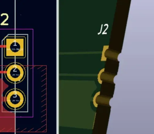
Also perform a visual review in both 2D and 3D viewers. Confirm that reference designators are readable, polarity marks are present, and no components collide mechanically.
A clean DRC that matches the fabricator's capabilities is one of the strongest predictors that the board will pass the manufacturer's own engineering review.
AIVON Manufacturing Tips for KiCad Layouts
Designing according to real fabrication requirements is the final step that turns a layout into a manufacturable product.
Confirm the PCB manufacturer's minimum trace width, spacing, hole size, and layer capabilities before you finish routing. Add stack-up notes and any special requirements (impedance control, specific surface finish, controlled depth drilling) directly in the board file or in a fabrication drawing.
When the layout and DRC are complete, generate the full manufacturing package: Gerbers, drill files, BOM, and pick-and-place data. With the AIVON KiCad plugin, engineers can move from the finished layout directly into quotation and ordering without manually re-packaging every file. This keeps the data consistent and reduces the chance of missing layers or incorrect parameters reaching the factory.
Designing inside the fabricator's process window from the beginning, then delivering a complete and verified file set, is the most reliable way to obtain first-pass success.
Following this structured layout process—preparation, thoughtful placement, rule-driven routing, thorough checking, and manufacturing-aware finalization—turns KiCad from a drawing tool into a practical path from schematic to reliable, producible PCB.
FAQ
Q1: How do I start a PCB layout in KiCad after finishing the schematic?
A1: Update the PCB from the schematic to import footprints and the netlist. Then open Board Setup to define the board outline, layers, and design rules that match your manufacturer before placing any components.
Q2: What are the most important design rules to set in KiCad for beginners?
A2: Set minimum track width, clearance, via size, and annular ring according to the fabricator's capabilities. Create net classes for power and signals so the router and DRC enforce the correct values automatically.
Q3: How should I place components in KiCad for better routing and signal integrity?
A3: Place connectors, crystals, and power parts first. Group related circuits, keep analog and digital sections separated, and locate decoupling capacitors close to the pins they serve. Good placement reduces trace length and via count.
Q4: When should I run DRC in a KiCad PCB layout?
A4: Run Design Rule Check after placement, after significant routing, and once more before generating manufacturing files. Fix every error and review warnings while changes are still easy to make.
Q5: How can I make sure my KiCad layout is ready for manufacturing?
A5: Design within the manufacturer's process limits, pass a full DRC with those rules loaded, generate complete Gerber, drill, BOM and pick-and-place files, and verify the package before ordering. Early confirmation of fab capabilities prevents late redesigns.
```