










From a fabrication standpoint, the choice between 1+N+1 and 2+N+2 HDI stackups is driven by routing density and via structure more than by layer count alone. A 1+N+1 structure uses one sequential build-up layer on each side of the core and remains the lower-cost, higher-yield option for many designs. A 2+N+2 structure adds a second build-up layer on each side, enabling finer escape from dense BGAs and more routing channels, but it increases process steps, registration risk, and unit cost.
Most shops recommend starting with 1+N+1 and only moving to 2+N+2 when the design cannot be routed or the BGA pitch forces additional microvia layers. Over-specifying 2+N+2 is one of the more common sources of unnecessary cost and longer lead time in HDI production.
Where 1+N+1 and 2+N+2 Stackups Separate
| Factor | 1+N+1 HDI | 2+N+2 HDI |
|---|---|---|
| Build-up layers per side | One | Two |
| Typical total layers | 6–10 (common) | 8–14 (common) |
| Routing density | Moderate to high | Higher – extra microvia layer frees more channels |
| BGA escape capability | Good for 0.5–0.8 mm pitch | Better for finer pitch and higher pin counts |
| Manufacturing complexity | Lower – one sequential cycle per side | Higher – two sequential cycles per side |
| Registration risk | Moderate | Higher with each additional build-up |
| Cost relative to each other | Baseline for HDI | 20–50 %+ higher depending on features |
| Typical applications | Many smartphones, modules, mid-density HDI | High-pin-count BGAs, ultra-compact designs |
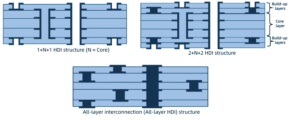
Decision Matrix for Stackup Selection
| If your priority is… | Better Choice | Why |
|---|---|---|
| Lowest HDI cost and highest yield | 1+N+1 | Fewer sequential cycles and lower process risk |
| Fine-pitch or high-pin-count BGA escape | 2+N+2 | Extra microvia layer provides additional routing channels |
| Fast prototype and stable production | 1+N+1 | Simpler process flow and wider process window |
| Maximum interconnect density in small form factor | 2+N+2 | Two build-up layers enable denser via structures |
| Moderate density with cost sensitivity | 1+N+1 | Usually sufficient without the extra cost of second build-up |
| Stacked microvias requiring more than one build-up depth | 2+N+2 | Supports deeper sequential via stacking |
Layer Structure and Routing Capability
In a 1+N+1 stackup the core (N) carries the main power and ground planes plus some signal layers, while a single build-up layer on each side provides the outer microvia connections and fine-line routing. This structure supports effective escape from many 0.5 mm and 0.65 mm BGAs when the via strategy is well planned. A 2+N+2 stackup adds a second build-up layer on each side, creating an additional microvia level. The extra layer significantly increases the number of available routing channels under and around high-pin-count packages.
From a stackup design perspective, 2+N+2 becomes necessary when a single build-up layer cannot provide enough escape routes or when stacked microvias must span more than one dielectric layer on each side. For many mid-density HDI boards, 1+N+1 remains fully capable and more economical.
Manufacturing Difficulty and Process Risk
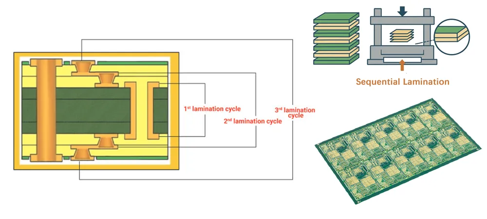
Each sequential build-up cycle multiplies registration, lamination, and laser-drill challenges. A 1+N+1 board typically requires one sequential lamination and laser-drill cycle per side. A 2+N+2 board requires two. The additional cycle increases the chance of misregistration, resin voids, and microvia plating defects. Yield models are more conservative for 2+N+2, and first-article inspection is more rigorous.
In the factory, 1+N+1 runs with a wider process window and higher first-pass yield. 2+N+2 occupies more specialized sequential capacity and demands tighter process control. This difference shows up clearly in both prototype turnaround and volume production stability.
Cost Differences in Real Production
Material cost is only part of the premium. The second sequential cycle adds laser drilling, additional lamination, plating, and inspection steps. As a result, 2+N+2 boards commonly cost 20–50 % more than comparable 1+N+1 boards of similar overall layer count, and sometimes more when via density is high. The cost is justified only when the extra routing capability is actually required.
At low to medium volumes the gap is especially noticeable because engineering and setup time for the more complex stackup is higher. At high volume the difference narrows but rarely disappears. Most fabricators will challenge a 2+N+2 specification if the design can be shown to fit within a 1+N+1 structure.
BGA Escape and High-Density Applications
Fine-pitch and high-pin-count BGAs are the primary drivers for moving from 1+N+1 to 2+N+2. With only one build-up layer, escape routing can become congested under large packages. The second build-up layer provides an additional microvia level and more real estate for signal breakout. Designs with 0.4 mm pitch or very high pin counts frequently require 2+N+2 or even higher structures.
For many consumer modules, wearables, and mid-range processors, 1+N+1 remains sufficient when via-in-pad and careful layer assignment are used. Jumping to 2+N+2 without a clear routing need adds cost without performance gain.
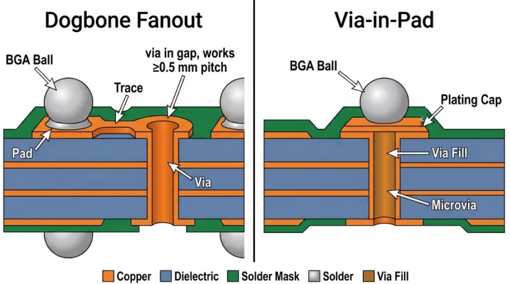
How PCB Factories Evaluate 1+N+1 vs 2+N+2
During DFM and CAM review the first questions focus on BGA pitch, pin count, and whether the design can be routed with a single build-up layer. If the answer is yes, 1+N+1 is strongly preferred. When stacked microvias or additional escape layers are required, the design is evaluated for 2+N+2 capability, including registration budget, dielectric thickness, and via aspect ratios.
Process risk rises with each sequential cycle. Factories look at historical yield data for similar structures and may recommend design adjustments—such as staggered instead of stacked microvias or redistribution of signals—to stay within 1+N+1. Panel utilization and test coupon requirements also increase slightly with 2+N+2 because of the tighter process controls needed.
In production planning, 1+N+1 offers more capacity flexibility and shorter lead times. 2+N+2 competes for sequential lamination and laser capacity that is often more constrained. This difference is visible in both prototype and volume scheduling.
Which Stackup Should You Choose?
Choose 1+N+1 if you:
- Can escape your BGAs and route the board with one build-up layer per side
- Need the lowest HDI cost and highest production yield
- Want faster prototype turns and more predictable lead times
- Are working with moderate-density modules or many consumer applications
- Prefer a wider process window and simpler manufacturing flow
Choose 2+N+2 if you:
- Must escape fine-pitch or high-pin-count BGAs that exceed 1+N+1 routing capacity
- Require additional microvia layers for stacked vias or higher interconnect density
- Are designing ultra-compact products where every routing channel matters
- Can accept the higher cost and longer process time for the density benefit
- Have confirmed that 1+N+1 cannot meet the electrical or mechanical requirements
In practice, many designs that initially appear to need 2+N+2 can be optimized back to 1+N+1 through better via planning, layer assignment, or selective use of via-in-pad. Always start with the simpler structure and escalate only when routing or form-factor constraints make it necessary. This approach keeps cost and process risk under control while still delivering the required density.
Frequently Asked Questions
Q1: Is 2+N+2 always better than 1+N+1 for high-density designs?
A1: Not always. 2+N+2 provides more routing channels and better fine-pitch escape, but many high-density boards can still be realized in 1+N+1 with careful via and layer planning. The extra structure should be used only when the additional density is actually required.
Q2: How much more does a 2+N+2 board typically cost?
A2: Expect a 20–50 % premium or more compared with a similar 1+N+1 design, driven by the additional sequential lamination, laser drilling, and process controls. The exact delta depends on via density, board size, and volume.
Q3: Can I use stacked microvias in a 1+N+1 stackup?
A3: Yes, but the stacking depth is limited by the single build-up layer. 2+N+2 allows deeper sequential stacking because of the second build-up dielectric on each side.
Q4: Which structure has better yield in volume production?
A4: 1+N+1 generally delivers higher and more stable yields because it involves fewer sequential cycles and a wider process window. 2+N+2 yield is more sensitive to registration and plating control.
Q5: When does BGA pitch force a move to 2+N+2?
A5: When escape routing under the package cannot be completed with one build-up layer, commonly seen with finer pitches (around 0.4 mm) or very high pin counts. Many 0.5 mm and larger packages can still be handled in 1+N+1.
Q6: Is it possible to mix 1+N+1 and 2+N+2 concepts on one board?
A6: In practice the overall stackup is defined as one or the other. However, designers can sometimes limit the second build-up features to only the densest regions while keeping the rest of the board simpler, provided the fabricator supports the resulting process flow.






