










Differential pair spacing in HDI is not a single number that can be set once and forgotten. It is the primary variable that sets differential impedance, controls coupling, and determines how much common-mode noise the pair will reject. When spacing varies along the route, or when it is chosen without regard to the stack-up and the surrounding features, the pair stops behaving as a controlled transmission line.
Most of the problems that appear in measurement or in the field can be traced to a small set of layout decisions made while routing. The CAD system will accept the changes. The signal will not.
Inconsistent Spacing and the Resulting Impedance Variation
Differential impedance is a direct function of the intra-pair spacing for a given trace width and dielectric height. A pair calculated for 100 Ω at 0.15 mm spacing will no longer be 100 Ω if the spacing opens to 0.25 mm for a short distance to clear an obstacle. The local impedance rises, a reflection occurs, and the differential signal sees a discontinuity.
In HDI the available routing channels are narrow. It is tempting to let the spacing breathe when the pair passes between vias or around a component pad. Each of those local openings creates its own impedance step. Multiple steps along a long channel accumulate into measurable return loss and deterministic jitter.
The same error occurs when the pair is necked down in width without a corresponding adjustment to spacing. Both dimensions must remain consistent with the target impedance. Changing one without the other moves the pair off the intended value.
Coupling Strength Versus Manufacturing Reality
Tighter spacing increases coupling. Strong coupling improves common-mode rejection and reduces the pair's sensitivity to external noise and to discontinuities in the return path. In dense HDI this is usually desirable. It also allows the pair to occupy less total width, which helps routing density.
The limit is set by the fab's ability to etch and register the two traces. When spacing approaches the minimum copper-to-copper clearance for the process, etch undercut and registration tolerance begin to consume the designed gap. The final spacing becomes variable from board to board, and the differential impedance follows that variation.
A practical floor for most commercial HDI is 0.10–0.125 mm edge-to-edge for outer-layer pairs when copper is 1 oz or less. Tighter values are possible on advanced lines with thinner copper and controlled etch, but they require process data, not just a brochure claim. Designing to the absolute minimum without margin produces pairs whose impedance is no longer under control.
Length Matching That Alters Spacing and Coupling
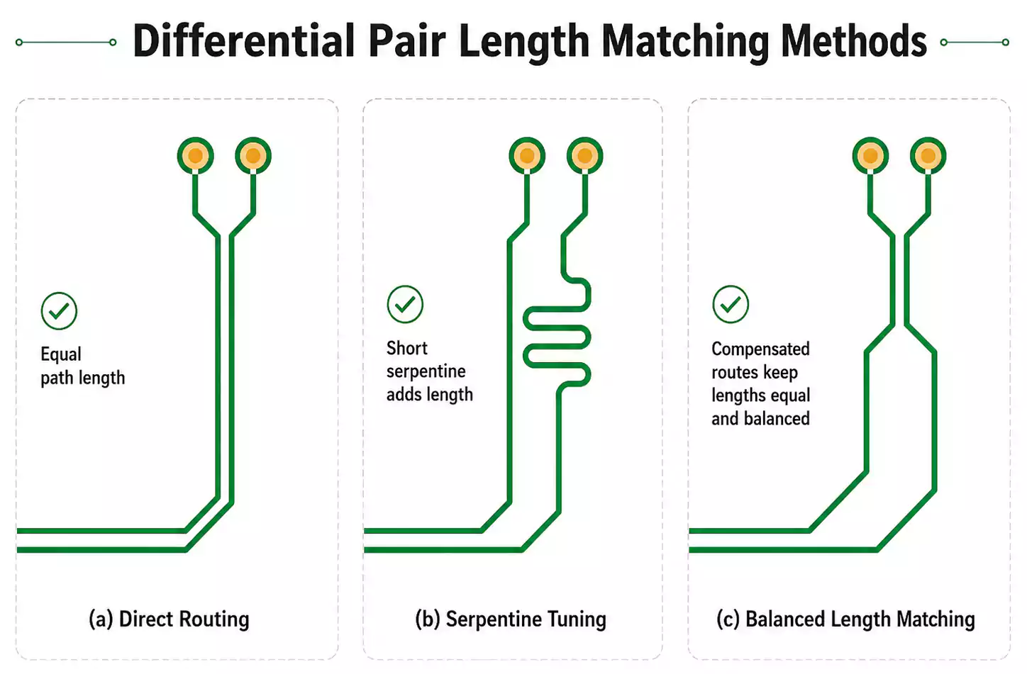
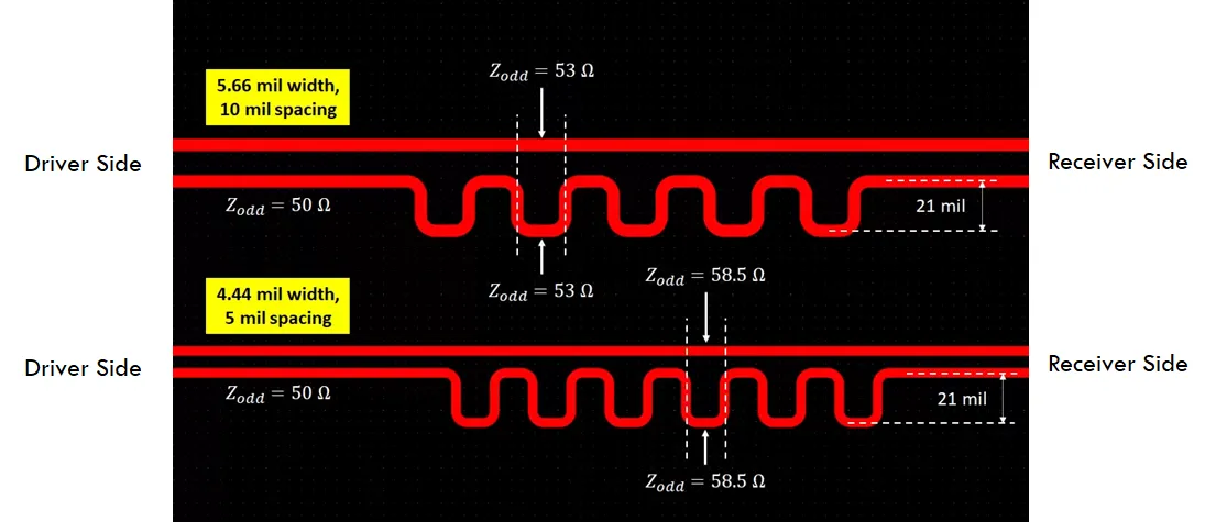
Length matching is required for timing, but the way the match is performed often destroys the spacing that was carefully set for impedance. Serpentine sections that increase the space between the two members of the pair, or that bring them closer, change the local coupling and therefore the local differential impedance.
The correct approach is to maintain the designed spacing through the matching geometry. Trombone or accordion sections should keep the intra-pair gap constant. When space forces a compromise, the matching should be done with the smallest possible deviation and the shortest possible length of altered spacing.
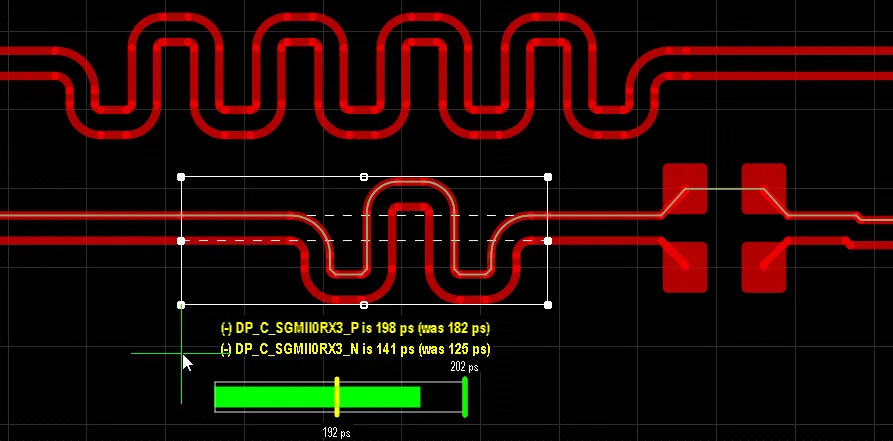
Matching one member of the pair by adding length while the other remains straight is acceptable only if the added length preserves spacing and does not introduce additional vias or reference changes. Any asymmetry in the matching geometry appears as residual intra-pair skew or as mode conversion.
Via Transitions and Layer Changes That Break the Pair
A differential pair is only as good as its via transition. When the pair changes layers, the two vias must be placed with the same spacing and symmetry that the traces use. Asymmetric via placement, different stub lengths, or unequal antipad clearances convert differential energy into common mode.
In HDI the microvia pair can be kept very tight, which helps preserve coupling through the transition. Through vias or longer buried vias introduce more discontinuity. Back-drilling must be applied equally to both members; residual stubs of different lengths are a common source of skew and mode conversion.
Reference plane changes are equally important. When the pair moves from one dielectric height to another, the spacing that produced 100 Ω on the first layer will not produce 100 Ω on the second. The spacing must be recalculated for the new stack-up, or the impedance will step at every layer transition.
Return path vias must also be considered. A tightly coupled pair still needs a nearby ground via for the return current when it changes layers. Placing that ground via asymmetrically relative to the signal pair re-introduces common-mode conversion.
Practical Rules That Keep HDI Differential Pair Spacing Stable
Choose the target spacing once for each layer type and hold it. Calculate the differential impedance for that geometry and for the actual dielectric height and copper weight. Do not adjust spacing ad-hoc to clear obstacles; clear the obstacles or change the routing path instead.
When a local deviation is unavoidable, keep it short and restore the designed spacing immediately. For length matching, preserve spacing through the matching geometry. For via transitions, treat the via pair as a continuation of the differential structure—same spacing, same symmetry, matched stubs.
On outer layers allow slightly more margin to the process minimum because etch variation is larger. On inner HDI layers the tighter spacing that comes with thinner copper and better registration can be used, provided the fab has demonstrated capability.
HDI differential pair spacing is a controlled geometric relationship, not a flexible keep-out that can be stretched when routing becomes difficult. Every intentional or accidental change in that spacing alters impedance, coupling, and mode conversion. The pairs that measure cleanly and pass compliance are the ones in which spacing was treated as a fixed design parameter from the first route to the final via transition.






