










Most HDI layout problems with microvias start the same way. The designer needs another escape route under a 0.4 mm or 0.35 mm BGA. The via diameter is already locked at 75 µm or 100 µm by the laser process. The only variable left is the capture pad. Shrink it a few tens of microns and the traces fit. Leave it larger and the density collapses.
That is the trade-off. The question is never "what is the theoretical minimum annular ring." It is "how thin can the copper ring become before the via stops being reliable under real registration, plating, and thermal stress."
Why Designers Keep Pushing Microvia Pads Smaller
Routing density is the driver. On a 0.4 mm pitch BGA the channel between two pads is already tight. A 250 µm capture pad leaves almost no room for a 50 µm trace plus clearance. Drop the pad to 200 µm and the trace fits. Drop it further and two traces become possible in some fan-out schemes.
The same pressure appears in via-in-pad structures and in stacked microvia columns. Every micron of annular ring removed is a micron of copper that can be used for routing or for tightening the stack. Designers who have just survived a dense escape on the previous revision will almost always try the same pad size again—or smaller.
That decision is rational at the layout stage. It only becomes a problem when the registration numbers and the plating process are ignored.
Registration Tolerance Is the Real Consumer of Annular Ring
Laser microvia registration is not a single number. It is the sum of several independent errors: copper feature registration on the target layer, laser-to-camera alignment, panel stretch after imaging, and sequential lamination movement. In a well-controlled process the combined 3σ tolerance is typically ±40 µm to ±60 µm. On less mature lines it can reach ±75 µm or worse.
If the design calls for a 50 µm annular ring and the drill lands 55 µm off center, the ring disappears on one side. The hole breaks out of the pad. On a single microvia that may still pass electrical test. On a stacked column the breakout becomes a stress riser that fails under thermal cycling or mechanical shock.
Most fabrication notes still list "minimum annular ring 50 µm" or "25 µm" as if those numbers are absolute. They are not. They are the residual copper after the worst-case registration has already been subtracted. Designers who treat the number as a hard design rule without adding the registration allowance end up with breakout.
What Happens When the Remaining Copper Ring Is Too Thin
Three failure modes appear repeatedly in reliability testing and in field returns.
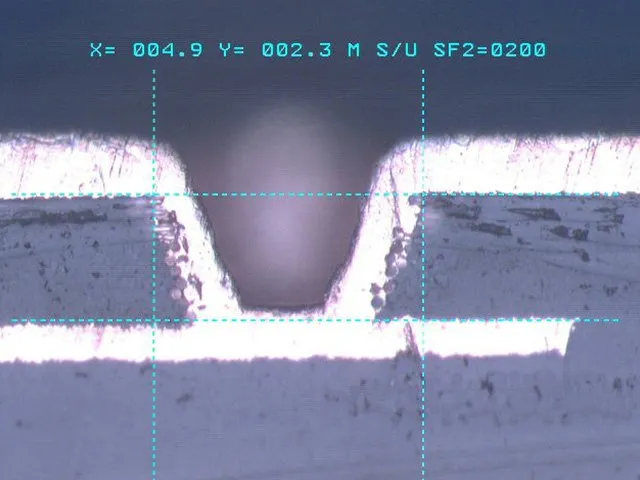
First is interfacial separation. The laser drills through the dielectric and stops on the capture pad. The subsequent electroless and electrolytic copper must bond to the remaining annular ring. When that ring is only 15–20 µm wide, the contact area is small. Thermal expansion mismatch between copper and resin pulls the via wall away from the pad during reflow or temperature cycling. The resistance rises gradually until the via opens.
Second is plating voids or thin plating at the knee. A narrow ring changes the local current density during electrolytic plating. The knee of the via receives less copper. Combined with any slight misalignment, the plated thickness on the critical interface drops below the 15–20 µm that most HDI reliability specs require.
Third is mechanical weakness under stacked microvias. Each additional microvia in a stack multiplies the stress concentration at the interface. A marginal annular ring that survives a single via often fails when three or four vias are stacked and the board sees 1 000 thermal cycles.
These are not theoretical concerns. They show up as intermittent opens after reflow, as increased resistance after thermal shock, and as via pull failures during microsection evaluation.
Practical Pad Size Calculation That Actually Works
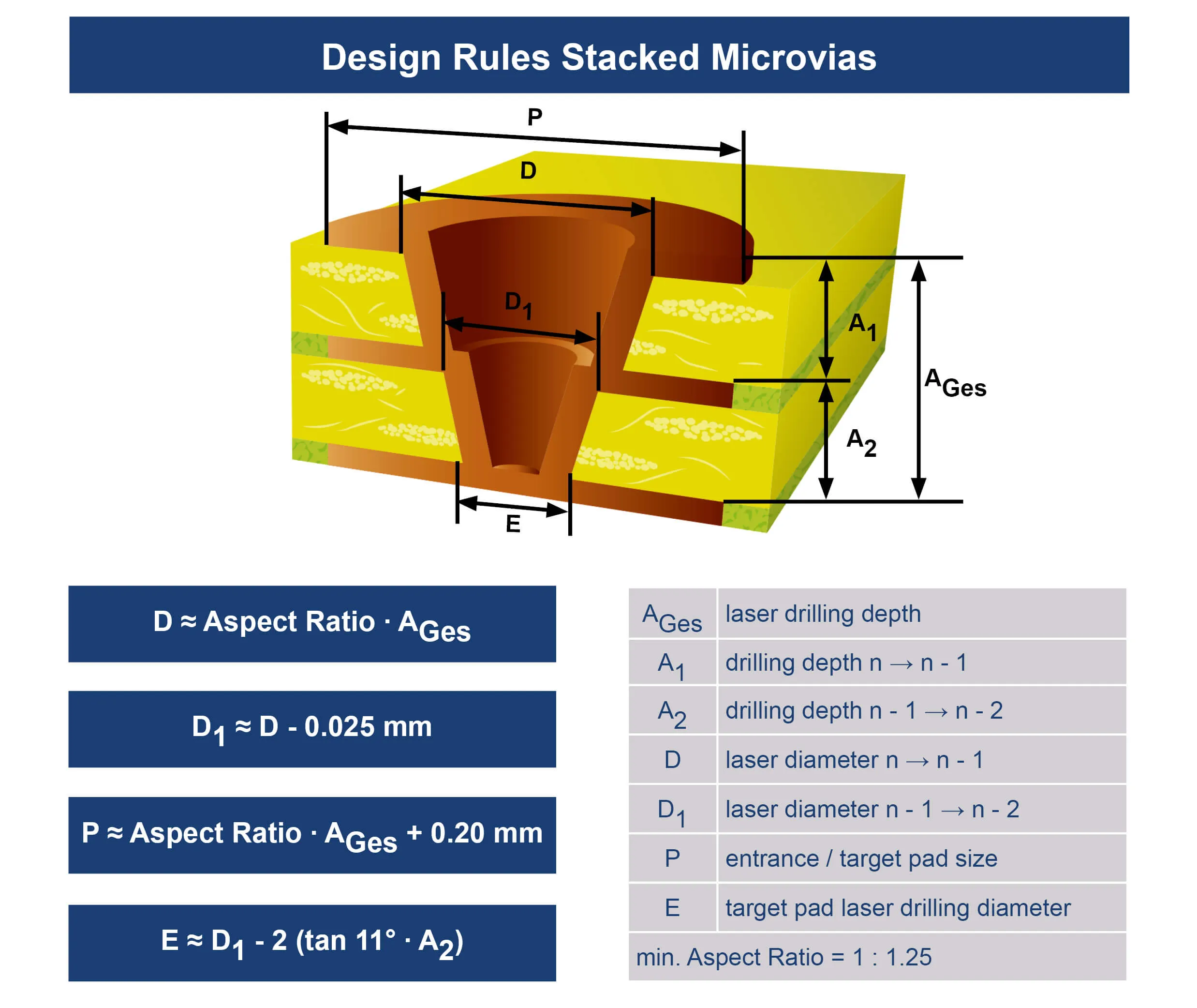
Start with the finished via diameter and the registration capability of the chosen fabricator, not with a generic IPC table.
A workable rule used on many production HDI boards is:
Capture pad diameter ≥ via diameter + 2 × (desired residual annular ring) + 2 × registration tolerance
For a 100 µm laser via, a target residual ring of 40 µm, and a process registration of ±50 µm, the pad becomes 100 + 80 + 100 = 280 µm. That number feels large to a density-focused designer, yet it is the size that consistently survives reliability testing.
When the fabricator can hold ±35 µm registration and the stack is only one or two microvias deep, the residual ring can be relaxed to 30 µm and the pad can drop to approximately 230–240 µm. Going below 25 µm residual copper on any capture pad in a stacked structure is rarely justified by the density gain.
Landing pads on the opposite side of the dielectric follow the same logic, but the registration stack-up is different because the laser stops on the copper rather than drilling through it. Many shops therefore allow a slightly smaller landing pad than capture pad for the same via diameter.
Routing Space Versus Reliability: The Real Compromise
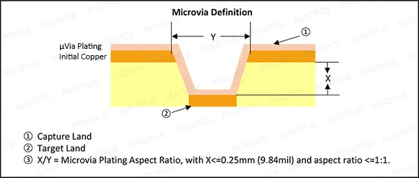
There is no free lunch. Reducing the capture pad by 40 µm can free a routing channel, but only if the fabricator's registration and plating process can support the resulting annular ring. When the process cannot, the board either fails reliability or requires a process change that costs more than the original density gain.
The practical approach is to fix the residual annular ring first—based on the number of stacked microvias and the expected thermal environment—then back-calculate the pad size using the fabricator's actual registration data. Only after that number is known should the layout attempt to squeeze traces between the pads.
If the resulting pad still blocks the required routing, the correct response is usually to move to a smaller via diameter, improve the registration process, or accept an extra layer of HDI. Shrinking the annular ring below the process capability is not a design solution; it is a reliability risk that will appear later.
In short, HDI microvia pad size is not a density number. It is the remaining copper after registration error has been paid. Design that residual ring first. Everything else follows.






