










Most HDI designs leave the CAD system with a registration number taken from the fabricator's capability table. The number is treated as a hard limit. Then the first prototype returns with microvia breakout, thin residual annular ring, or layer-to-layer shift that the design never budgeted for.
HDI registration tolerance is not a single value. It is the sum of several independent process errors that accumulate across sequential lamination, laser drilling, and imaging steps. Designers who release a board without checking how those errors stack up against the actual pad margins are gambling with reliability.
Layer-to-Layer Registration Is a Stack of Separate Errors
In conventional multilayer boards the dominant registration term is inner-layer imaging-to-lamination shift. In HDI the list is longer. Each sequential build-up cycle adds its own contribution: copper feature registration on the target layer, laser-to-camera alignment, dielectric thickness variation that affects scale factors, and outer-layer imaging after the final press.
A fabricator that quotes ±50 µm registration usually means the combined result under ideal conditions. Real panels see additional movement from material stretch, press pressure variation, and thermal history. When three or four HDI layers are built sequentially, the cumulative shift at the outermost microvia can easily exceed the quoted number.
Designers who apply the same ±50 µm allowance to every interface in a stacked microvia column are already under-estimating the total error budget.
Microvia-to-Pad Alignment Absorbs the Entire Stack-Up
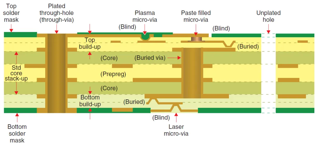
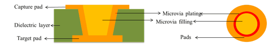
The laser drills to a copper target. The remaining copper around the hole is the residual annular ring. That ring is what is left after every registration error has already been subtracted. If the design pad was sized for a 40 µm residual ring and the process delivers 55 µm of total shift, the ring disappears on one side.
Breakout on a single microvia may still pass continuity. On a stacked column the same breakout becomes a stress concentration. Thermal cycling and mechanical shock open the interface. The failure appears weeks or months later as intermittent resistance or complete open.
Capture pads and landing pads experience different portions of the error stack. The capture pad sees the laser alignment plus the target-layer copper registration. The landing pad on the opposite side of the dielectric sees a different combination. Treating both pads with the same margin is a common shortcut that under-protects one of the interfaces.
Pad Margin That Actually Survives Cumulative Process Deviation
The only reliable way to size a microvia pad is to start from the residual annular ring required for reliability, then add the full expected registration stack-up. A 30–40 µm residual ring is a practical target for most single and double microvia stacks when the thermal environment is moderate. Stacked columns of three or more usually need 40–50 µm residual copper to survive extended cycling.
If the fabricator's true process capability is ±45 µm at the critical interface, the pad diameter must absorb that full amount on both sides plus the residual ring. Designers who use only the residual ring number and ignore the registration term consistently produce boards that sit on the edge of breakout.
The same calculation applies to through-via capture pads and to any feature that must maintain copper continuity across sequential layers. The principle is identical: residual copper after worst-case shift is the only number that matters for reliability.
Process Steps That Quietly Inflate the Total Error
Several steps contribute more error than most design rules acknowledge. Lamination scale factors change with dielectric type, copper coverage, and press cycle. Laser cameras that align to etched copper features inherit the etch undercut and the imaging registration of that layer. Outer-layer imaging after the final sequential press sees the cumulative stretch of every previous cycle.
Material choice matters. Some high-speed laminates exhibit larger dimensional change than standard FR-4 type materials under the same press conditions. Using the registration numbers from a previous FR-4 job on a new low-loss stack is a frequent source of unexpected shift.
Panel size and coupon location also affect the result. Registration measured near the panel center is almost always better than the numbers seen near the edges. Designs that place critical microvia columns near the panel periphery without extra margin are more likely to see breakout.
Registration Checks Worth Completing Before Release
Before the design is released, the registration budget should be verified against the actual process, not against a generic table. Ask the fabricator for the measured 3σ registration at each critical interface for the specific material and sequential stack being used. The number for a first HDI layer is rarely the same as the number for the third sequential layer.
Recalculate residual annular ring for every microvia type using those numbers. Confirm that stacked columns still retain the minimum residual copper after the worst-case cumulative shift. Check that capture pads and landing pads have been sized independently if their registration paths differ.
Verify that any via-in-pad or via-under-pad structures still maintain copper continuity under the same shift. Confirm that the design does not place critical microvia arrays near panel edges without additional margin. Finally, confirm that the fabrication notes explicitly state the registration assumption used so the CAM engineers can flag any discrepancy.
HDI registration tolerance is manageable when it is treated as a cumulative process reality rather than a single data-sheet number. The designers who consistently avoid breakout and thin-ring failures are the ones who force the error budget into the open before the files leave the system. Everything after that is just manufacturing execution.






