










In HDI layouts the space around a via is not free real estate. A keepout zone exists because the via itself creates mechanical, thermal, and assembly constraints that components cannot tolerate. When a part is placed too close, the result is solder joint voids, tombstoning, wicking, or inspection failures. The keepout is not an arbitrary CAD rule. It is the minimum distance required for the assembly process and the finished joint to remain reliable.
Most designers define HDI via keepout only after placement problems appear. That is backwards. The keepout should be established during stack-up definition and component placement so that routing density does not force parts into restricted areas later.
What a Via Keepout Zone Actually Restricts
A via keepout is the region surrounding a via pad or drilled hole where component bodies, component pads, and sometimes copper features are prohibited. The restriction is driven by three practical limits: the physical size of the pick-and-place nozzle, the behavior of solder paste and flux during reflow, and the outgassing or stress that occurs at the via itself.
In HDI the via is often smaller and the surrounding copper tighter than on conventional boards. That does not eliminate the keepout. It only changes the distance. Microvias still require clearance for assembly access and for reliable solder joints on nearby pads. Through vias and via-in-pad structures impose additional restrictions because of their larger thermal mass and potential for solder wicking.
The keepout is measured from the edge of the via pad or the finished hole, depending on the fab and assembly house definition. Mixing the two measurement methods is a common source of later confusion.
Component-to-Via Distance and Assembly Reliability
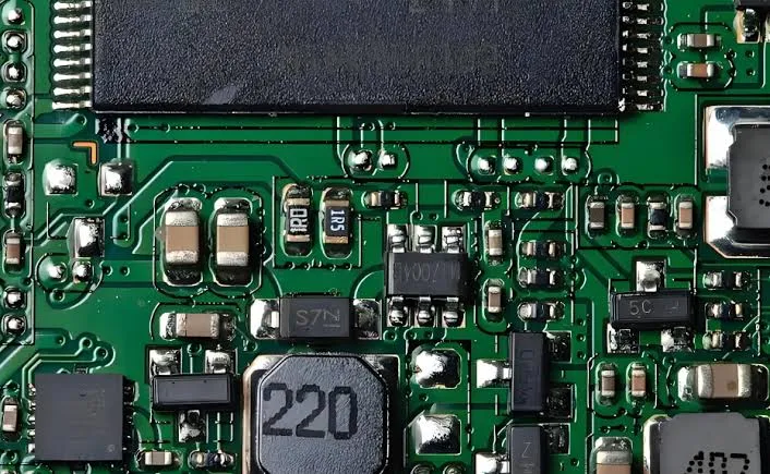
The most frequent failure mode is solder joint degradation on a component pad that sits too close to an open via. During reflow the via can act as a thermal sink or as a path for solder wicking. Paste is drawn away from the component pad, leaving a starved joint. In the opposite case, flux and volatiles from the via outgas directly under or beside the component, creating voids or shifting the part.
For small chip components the practical minimum body-to-via clearance is typically 0.3–0.5 mm on outer layers when the via is not filled and capped. Tighter distances are possible with filled and plated-over microvias, but only when the assembly process has been qualified for that condition. Fine-pitch QFN or BGA packages near vias require additional margin because the nozzle and the vision system need clear space, and because any tilt or void is harder to inspect.
Through vias under or immediately adjacent to components are especially problematic unless they are fully filled and planarized. Open barrels provide a low-resistance path for solder to leave the joint. The keepout around such vias should be treated as larger than the keepout around a capped microvia.
Restrictions Around Via Pads and Via-in-Pad Features
When the via is intentionally placed in a component pad (via-in-pad), the keepout rules change. The via must be filled, capped, and planarized so that the pad surface remains flat for soldering. Any residual dimple or incomplete fill becomes a void initiation site. In that case the keepout is no longer a lateral distance; it is a process requirement on the via itself.
For non-via-in-pad situations the component pad edge should maintain a clear gap from the via pad edge. Typical production values fall in the 0.15–0.25 mm range for HDI outer layers when copper is 1 oz or less. Closer spacing risks copper bridging during etch or solder mask dam failure between the two pads.
Inner-layer vias have different constraints. There is no assembly concern, but registration and etch still require a minimum copper-to-copper clearance. The keepout on inner layers is therefore driven by fabrication capability rather than placement or reflow.
Assembly Space and Inspection Access
Beyond the solder joint itself, the keepout must leave room for the pick-and-place process. Nozzles, especially for small parts, need a clear approach path. Vision systems used for alignment can be confused by nearby via pads or copper features that create high-contrast edges. Dense HDI areas with many microvias can reduce the effective keepout if the vias are filled and the surface is planar, but open vias still demand extra space.
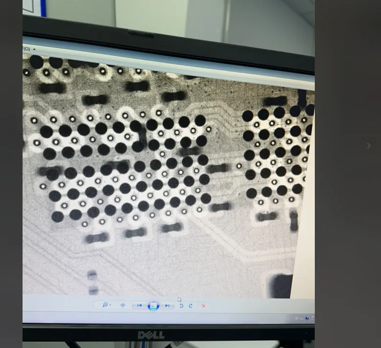
Automated optical inspection and X-ray also benefit from clearance. A component placed directly against a via cluster can hide voids or make side-view inspection impossible. In high-reliability work the keepout is often increased simply to guarantee that every joint remains visible and measurable.
Defining Keepouts Early in the Layout Process
The most effective way to manage HDI via keepout is to establish the rules before component placement begins. Once the stack-up and via types are fixed, the assembly house and fab capability determine the minimum distances. Those distances are then entered as CAD rules or keepout shapes around every via.
Different via types need different keepouts. Microvias that are filled and capped can run tighter. Through vias that remain open need larger zones. Via-in-pad locations need process notes rather than lateral keepouts. Treating every via with a single global number either wastes density or creates hidden assembly risk.
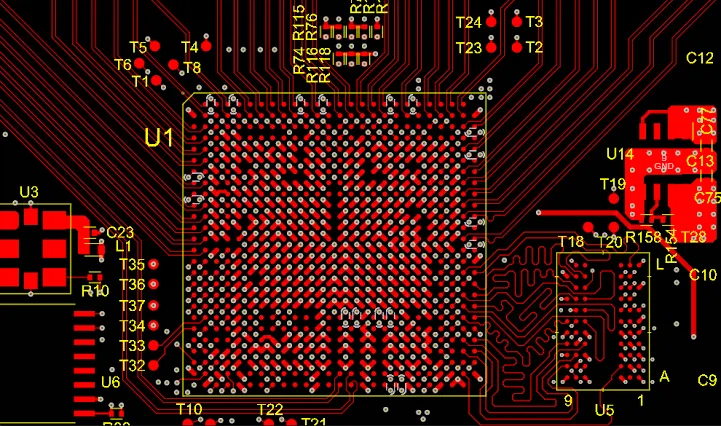
During placement, high-pin-count devices and fine-pitch parts should be positioned first with their via keepouts visible. Routing then fills the remaining space. When a via must sit closer than the preferred keepout, the designer should confirm with the assembly process that the specific combination of via fill, pad geometry, and component type has been qualified.
Practical Values That Hold in Production
For typical commercial HDI the following starting points are realistic. Open microvia to component body: 0.4 mm. Filled and capped microvia to component pad edge: 0.15–0.20 mm. Through via to any component: 0.5 mm or greater unless the via is filled. These numbers assume standard reflow and inspection processes. Tighter values require process qualification data from the specific assembly line.
The keepout is not only a lateral distance. It is also a statement about via construction. An open barrel near a component pad is a different risk than a planar, copper-capped microvia. Design rules that ignore the via fill condition will either over-constrain the layout or allow failures that only appear after reflow.
HDI via keepout exists to protect the solder joint and the assembly process. When the zone is respected, components solder cleanly and remain inspectable. When it is violated, the board may still leave the fab, but the assembly yield and long-term joint reliability become the next problems to solve. Defining the keepout early and matching it to the actual via construction is the only reliable way to keep both density and manufacturability under control.






