In HDI work the clearance between a via and adjacent copper is rarely the number that looks correct in the CAD system. It is the number that remains after etch undercut, drill or laser registration, and outer-layer pattern shift have all taken their share. When that remaining isolation drops below the process floor, the result is not a clean open. It is intermittent shorts, copper bridging, or scrap that only appears after the panels have already been plated and etched.
Most designers treat HDI via to copper clearance as a simple keep-out rule. The rule is applied once at layout and then forgotten. That approach works until the board reaches CAM. Then the questions start.
How Designed Clearance Shrinks on the Fabrication Floor
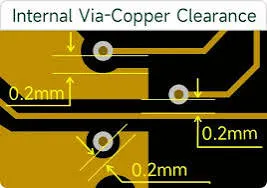
A 0.10 mm clearance drawn in the layout is not what the etch process sees. Copper etching removes material from the sidewalls of every feature. On fine-line outer layers the lateral undercut commonly runs 0.015–0.025 mm per side depending on copper thickness and etch chemistry. That alone converts a nominal 0.10 mm gap into something closer to 0.06–0.07 mm.
Registration adds the next cut. Laser-to-copper registration on HDI layers is typically held to ±0.05 mm or better on advanced lines, but the cumulative stack—inner-layer registration, laser positioning, and outer-layer artwork—can easily consume another 0.03–0.05 mm of the original clearance. The via pad or the drilled hole edge ends up closer to the neighboring copper than the designer ever intended.
When the via sits next to a large copper plane the problem is worse. Plane edges are often drawn with intentional etch compensation already applied. If the via clearance was measured to the compensated edge rather than the final copper edge, the actual isolation after processing is even smaller.
Where Short Circuits Actually Form
The short does not always appear as a solid copper bridge visible under the microscope. More often residual copper filaments or partially etched residues remain in the narrowed gap. These residues can survive cleaning and plating, then create high-resistance or intermittent connections that pass electrical test but fail later under humidity or thermal stress.
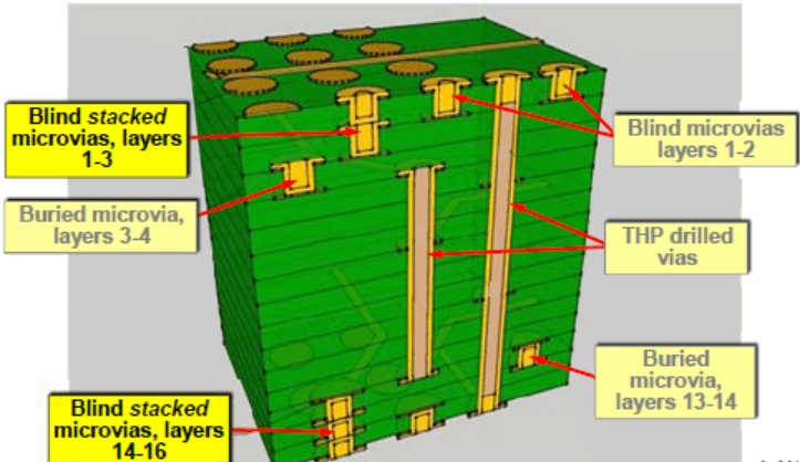
In sequential build-up HDI the risk multiplies. A microvia that is already close to a copper feature on its capture layer can be driven even closer by the registration of the next dielectric and copper foil. Stacked or staggered microvias near plane edges are frequent offenders because each layer adds its own registration tolerance.
Through vias that transition between HDI layers and conventional cores face the same issue on the outer layers. The annular ring is small, the copper pour is dense, and the clearance that looked adequate in the layout becomes marginal once the outer-layer etch factor is applied.
What CAM Engineers Flag Most Often
When the files reach CAM the first automated checks look for via-to-copper clearances below the fab's published minimum. For many HDI-capable shops that number sits between 0.075 mm and 0.10 mm on outer layers and slightly tighter on inner HDI layers if the process is qualified. Anything under the limit generates an engineering query.
The more subtle flags involve clearances that are nominally acceptable but sit next to large copper areas or isolated copper islands. CAM will often ask whether the copper is intentional and whether the isolation is required for electrical reasons. If the designer cannot justify the tight spacing, the request is usually to open the clearance or to pull the copper back.
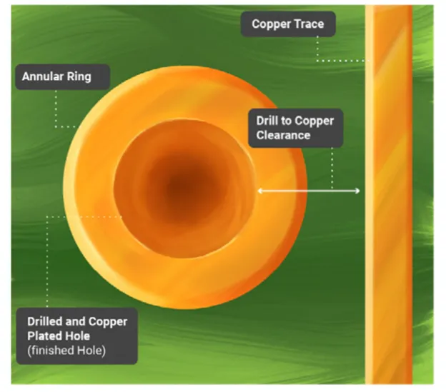
Another common note concerns the measurement method itself. Some designers measure from the edge of the finished hole; others measure from the edge of the pad. CAM software measures from the copper edge of the pad or the plated hole wall after etch compensation. Mismatches in that definition produce false confidence in the layout and real problems on the production floor.
Practical Clearance Values That Hold Up in Production
For most production HDI the safe starting point for via-to-copper clearance on outer layers is 0.15 mm when the copper is 1 oz or less and the etch process is standard. That value absorbs typical undercut plus registration stack-up and still leaves usable isolation. On advanced lines with tight registration and controlled etch the number can be reduced to 0.10 mm, but only when the fab has demonstrated the capability on similar constructions.
Inner HDI layers can sometimes run tighter because the dielectric is thinner and the registration is laser-based. Even then, 0.10 mm remains a practical floor for most commercial work. Going below that requires process qualification data, not just a brochure claim.
When density forces tighter spacing the correct response is usually to pull the copper back rather than to shrink the clearance. Creating a local keep-out or a thermal relief style opening around the via restores isolation without forcing the entire plane to move. In high-density areas this is often the only practical way to keep both routing density and manufacturability.
Design rules should also distinguish between connected and non-connected copper. Clearance to a copper feature that shares the same net can be zero (or defined by the annular ring). Clearance to any other net must carry the full process tolerance. Mixing the two definitions is a frequent source of later CAM questions.
Building Margin Into the Design Rule
The most reliable approach is to set the CAD rule 0.025–0.05 mm larger than the fab's stated minimum HDI via to copper clearance capability. That extra margin covers normal process variation across a production lot and across multiple fabricators if the design is dual-sourced.
When the stack-up includes both laser microvias and mechanical vias, apply the tighter rule to the entire design rather than maintaining separate values. Mixed rules create inconsistencies that are easy to miss during layout and hard to defend during CAM review.
Finally, document the measurement method. State clearly whether clearance is measured from the finished hole edge, the plated wall, or the outer edge of the pad. CAM engineers will use their own definition; matching it in the design notes eliminates a common source of back-and-forth.
HDI via to copper clearance is not a theoretical minimum. It is the isolation that survives etch, registration, and plating. Designing to the absolute process floor leaves no room for the real variation that every production panel experiences. The boards that run cleanly are the ones that were laid out with that variation already accounted for.