










Connector pin density is one of the strongest drivers of HDI technology choice. When the pitch drops and the pin count rises, the number of routing channels available between pins shrinks faster than the number of signals that must escape. At that point conventional through-via fan-out becomes impractical. The board either gains layers, adopts microvias, or both.
The decision is not aesthetic. It is arithmetic. The available space between pins, the minimum trace and space the fab can hold, and the number of signals that must leave the connector determine whether a design can stay with standard vias or must move to sequential build-up HDI.
How HDI Connector Pin Pitch Changes Available Routing Channels
Pitch sets the maximum number of traces that can pass between adjacent pins. On a 0.8 mm pitch connector the gap is relatively generous. On 0.5 mm or 0.4 mm pitch the gap shrinks to the point where only one or two fine traces can fit after accounting for pad size, annular ring, and clearance.
High pin count multiplies the problem. A connector with 100+ pins on fine pitch may require dozens of signals to escape from the inner rows. Each successive row blocks more of the available channels. Without additional layers or the ability to drop to deeper layers quickly, the inner pins become unroutable.
This is the point at which connector pin density HDI decisions are forced. The layout can no longer treat the connector as a standard component that is fanned out with through vias on a four- or six-layer board.
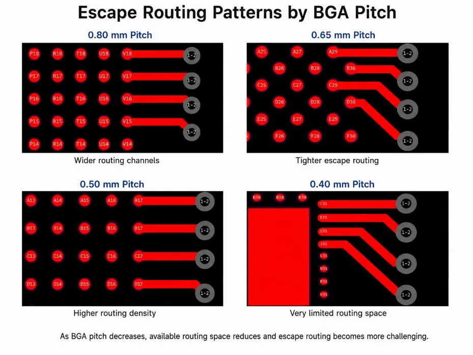
Why HDI Connector Routing Becomes Difficult at High Density
A through via occupies space on every layer. In a dense connector field the vias from outer rows block the routing channels needed by inner rows. The result is a cascading loss of escape paths. Designers respond by increasing layer count, but each added layer still carries the via keepout from all the pins above it.
Via-in-pad can recover some space, yet on fine-pitch connectors the pad itself is already small. Adding a via and the required annular ring or capture pad further reduces the remaining copper for soldering and can create assembly risks if the via is not properly filled and planarized.
At a certain density the through-via approach consumes more routing real estate than it provides. That is the practical threshold where HDI microvia technology becomes the lower-cost and higher-yield solution.
Building an HDI Routing Strategy Around Microvias and Layer Count
Microvias change the escape arithmetic. A laser microvia can connect the surface pad to layer 2 without occupying space on layers 3 and below. The signal can then route on layer 2 or drop again with another microvia. Inner pins gain escape paths that through vias would have blocked.
The number of HDI layers required is set by how many signals must be extracted from the densest region of the connector. A simple single-level microvia (1+N+1) is often sufficient for moderate density. Higher pin counts or tighter pitches push the design toward two or more sequential build-up layers on each side.
Each additional HDI layer adds cost, but it also multiplies the number of available routing channels. The correct layer count is the minimum that allows every signal to escape without violating minimum trace width, spacing, or via registration rules. Adding layers beyond that point is usually unnecessary.
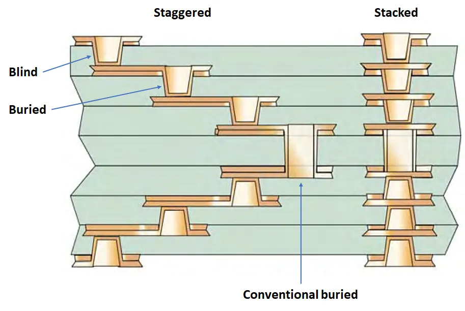
How HDI Connector Via Placement Supports Reliable Fan-Out
Not every pin needs the same via treatment. Ground and power pins can often share vias or use larger through vias outside the densest field. High-speed signal pins usually require dedicated microvias placed to preserve differential spacing and minimize stub length.
Via-in-pad is attractive for the tightest pitches because it eliminates the dog-bone breakout and frees the channel between pads. It demands filled and capped vias so the pad surface remains solderable. When the process cannot support via-in-pad at the required pitch, a short dog-bone to a nearby microvia is the next option, provided the dog-bone length does not create an excessive stub or impedance discontinuity.
The total via count under the connector should be minimized to reduce registration risk and copper balance issues. Clustering too many microvias in a small area can create local dielectric stress and make sequential lamination more difficult.
Planning HDI PCB High Density Routing From the Connector Outward
High-density connectors should be placed and escaped first. The rest of the board is then routed around the escape field. Defining the required HDI PCB layer count and via strategy before general placement prevents later discoveries that the connector cannot be fanned out on the chosen stack-up.
Keepout zones around the connector must account for the fan-out vias and the first routing channels. Component placement too close to the connector field simply relocates the density problem. High-speed pairs should be assigned to the layers and via structures that preserve their spacing and minimize layer transitions.
When multiple high-density connectors are present, their escape fields must be coordinated so that they do not compete for the same routing channels or via resources on the critical HDI layers.
Choosing the Right HDI Routing Approach for Actual Connector Density
Not every connector requires full HDI. A moderate pin count on 0.8 mm pitch can often be escaped with through vias and a modest layer count. The transition to connector pin density HDI becomes necessary when the combination of pitch and pin count leaves insufficient channels after minimum trace/space and via keepouts are applied.
The correct approach is to calculate the required number of escape routes, compare it with the available channels on the proposed stack-up, and only then decide on microvia count and layer count. Over-specifying HDI adds cost. Under-specifying it produces an unroutable board or a board that only routes by violating clearance and impedance rules.
Connector pin density sets the minimum technology floor for the entire design. Once that floor is acknowledged and the escape strategy is fixed, the remaining routing decisions become straightforward. When the density is ignored until late in layout, the only remaining options are expensive layer additions or compromised signal integrity. The boards that route cleanly are the ones in which the connector's pin density was allowed to dictate the HDI approach from the start.
FAQ
Q1: What is an HDI connector in a high-density PCB design?
A1: An HDI connector is a connector interface used in a PCB design where high pin density and limited routing space require advanced interconnection technology. Its fine pitch can reduce available escape channels, making conventional through-via fan-out difficult. HDI techniques such as microvias, sequential build-up, and via-in-pad structures can provide additional routing capacity around dense connector interfaces.
Q2: How does HDI PCB high density routing handle fine-pitch connectors?
A2: HDI PCB high density routing manages fine-pitch connectors by increasing the number of usable routing channels within a limited area. Designers may use microvias, finer trace geometries, additional build-up layers, and optimized via placement to escape connector pins efficiently. The required approach depends on connector pitch, pin count, fabrication capabilities, signal requirements, and the available PCB stack-up.
Q3: When does a connector require HDI routing?
A3: A connector may require HDI routing when its pin pitch and pin count leave too few channels for practical through-via fan-out. Designers should compare the available escape routes with trace-and-space capabilities, via dimensions, and layer availability. If conventional vias consume excessive routing space or force an impractical layer count, microvia-based HDI routing becomes a more suitable approach.
Q4: Why are microvias important for HDI connector routing?
A4: Microvias are important for HDI connector routing because they occupy less board area and can provide short vertical transitions between adjacent layers. This allows signals to escape dense connector fields without blocking as many routing channels as conventional through-vias. Microvias can also support via-in-pad and sequential build-up structures, giving designers more flexibility when routing fine-pitch, high-pin-count connector interfaces.
Q5: How does HDI routing affect connector layer-count decisions?
A5: HDI routing and layer count are closely connected because insufficient routing channels around a dense connector can force additional signal layers. Designers typically establish the connector escape strategy first, then determine how many build-up and core layers are needed. A balanced approach considers routing capacity, impedance requirements, fabrication limits, registration tolerance, reliability, and the cost impact of additional HDI layers.






