










FPC outline design is not just drawing a contour in CAD. The outline is the final cut that defines every edge of the flexible circuit. Get it wrong and the laser or the router leaves defects that no amount of electrical testing will catch until the part is flexed or assembled.
Most problems come from treating the outline like a rigid-board contour. Flexible PCB laser cutting and mechanical routing have different physical limits. Sharp internal corners and missing fillets are the two most common sources of scrap and reliability issues.
Why Internal Right Angles and Sharp Corners Are Difficult to Process
An internal right angle or acute corner creates a stress concentration and a process limitation at the same time.
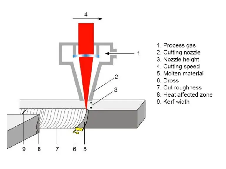
In laser cutting the beam has a finite diameter and a heat-affected zone. When the path makes a sharp internal turn, the laser dwells longer at the corner or the energy distribution becomes uneven. The result is often local overheating, carbonization, or incomplete separation of the polyimide. Thin copper near that corner can also be damaged by the extra heat.
Mechanical routing is even more constrained. The router bit has a physical radius. It cannot produce an internal corner sharper than its own radius. A 1 mm bit will leave a 0.5 mm minimum internal radius whether the designer drew a sharp corner or not. Attempting to force a sharper feature requires multiple passes, smaller tools, or secondary operations—all of which raise cost and risk of tearing the flexible material.
Sharp external corners are usually acceptable. Sharp internal corners are not. The distinction matters.
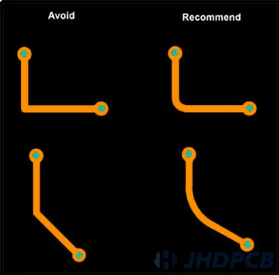
How Rounded Corners Improve Cutting Quality and Reliability
Adding a fillet to every internal corner does three practical things.
First, it matches the natural capability of both laser and mechanical processes. The cut path stays continuous and the energy or tool engagement remains consistent. Second, it removes the geometric stress riser. Flexible circuits are repeatedly bent. A sharp internal corner becomes a crack initiation site under cyclic flexing. A smooth radius distributes the stress. Third, it improves yield. Less carbonization, fewer tears, fewer parts rejected for outline defects.
The radius does not need to be large. A 0.5 mm internal radius is sufficient for most laser-cut FPCs. For thicker stacks or higher-reliability applications, 0.8 mm to 1.0 mm is safer. External corners can remain sharp or receive a small break; the critical locations are the internal ones.
Designers sometimes omit fillets to save a fraction of a millimeter in packaging. That saving is almost always lost later in scrap or field failures.
Laser Cutting versus Mechanical Routing Differences
Flexible PCB laser cutting and mechanical routing are not interchangeable. Each imposes different outline rules.
Laser cutting is non-contact. It can produce finer features, narrower slots, and tighter overall tolerances on the outline. Minimum internal radius is still limited by beam focus and heat, but it can be smaller than a typical router bit. Laser also creates a heat-affected zone and potential carbon residue that must be managed. Complex contours with many direction changes are handled well as long as internal corners are filleted.
Mechanical routing uses a spinning bit. Tool diameter sets the minimum internal radius and the minimum slot width. The process is slower for complex outlines and can leave burrs or mechanical stress in the polyimide. It is less common for high-volume FPC outlines but still used for certain rigid-flex sections or thicker constructions. When routing is the process, the designer must design to the actual tool radius that will be used—usually 0.5 mm or larger internal fillets.
Mixed processes also occur. Some panels are laser-cut for the fine outline and then mechanically separated or scored. The outline design must satisfy the more restrictive of the two methods at every feature.
Core FPC Outline Design Rules That Reduce Scrap
Several practical rules keep FPC outline design inside the process window.
Provide a minimum internal corner radius of 0.5 mm for laser cutting; increase to 0.8–1.0 mm when the stack is thick, the copper is heavy, or reliability requirements are high. Never rely on a sharp internal corner.
Keep copper and coverlay openings away from the final outline by the recommended edge clearance (typically 0.3 mm or more for laser). The outline cut and the copper features interact; they are not independent.
Avoid extremely narrow necks or slots that approach the kerf width or tool diameter. A slot that is only marginally wider than the laser kerf will show incomplete cuts or excessive heat damage at the ends.
Design the outline as a continuous closed path with consistent direction changes. Sudden reversals or overlapping segments create dwell points that overheat the material.
When the part has both rigid and flexible sections, define the outline transition carefully. Abrupt changes in material thickness at the cut line increase the chance of incomplete separation or tearing.
If the outline includes tabs or break-away features for panelization, size those features so they can be cleanly removed without damaging the adjacent flexible area. Sharp internal corners at tab roots are a frequent source of field cracks.
Common Design Choices That Create Outline Problems
Copying a rigid PCB outline style is the most frequent error. Rigid boards are often routed with larger tools and can tolerate sharper internal features because the material is thicker and more rigid. FPC polyimide does not forgive the same geometry.
Another common choice is maximizing every millimeter of usable area by pushing internal corners to zero radius. The packaging gain is real; the process and reliability cost is usually larger.
Designers also sometimes ignore the actual fabrication method. A contour that is acceptable for a slow, high-precision laser may fail on a high-speed production laser or on a mechanical router. Confirming the intended outline process before finalizing the radii is essential.
Practical Checks Before Releasing the Outline
Measure every internal corner radius in the final outline layer. Do not rely solely on the CAD constraint; verify the actual geometry that will be exported.
Confirm that the outline path is a single continuous contour without self-intersections or overlapping segments. Laser and router toolpaths both degrade when the geometry is unclean.
Check the relationship between the outline and nearby copper, coverlay, and stiffener edges. The cut must leave adequate clearance on all of them.
If the part will be laser-cut, ask the fabricator for their preferred minimum internal radius and kerf compensation. If it will be mechanically routed, obtain the actual tool diameter that will be used and design to that radius.
These checks take minutes. Fixing an outline after the first article fails takes days and usually requires a new panel.
Engineering Takeaway
FPC outline design must match the physics of the cutting process. Sharp internal corners create heat and tool problems for flexible PCB laser cutting and are geometrically impossible for mechanical routing without secondary work. Proper fillets remove those problems, improve yield, and increase flex life.
Design the outline with process-capable internal radii, maintain copper-to-edge clearance, and verify the actual fabrication method. Those three steps keep the contour inside the manufacturing window and prevent the most common outline-related defects on flexible circuits.






