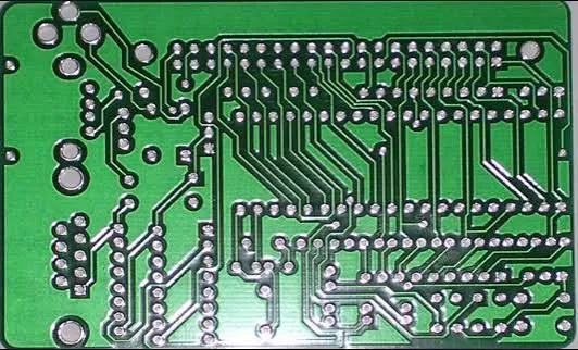
BGA pitch is one of the fastest ways to push a board into higher HDI cost brackets. Not the package size itself, not the pin count alone. The pitch. Once the center-to-center distance drops below roughly 0.5 mm, the escape geometry changes the stack-up, the via architecture, and the process window in ways that show up immediately on the fab quote.
Most designers reach for finer pitch because the silicon or the module forces it, or because board real-estate is already tight. The cost impact is secondary until the CAM team starts marking up the DFM notes.
How Pitch Directly Shrinks the Escape Channel
At 0.8 mm pitch a typical 0.45–0.50 mm pad still leaves enough room between pads for one or two 75–100 µm traces plus clearance. Fan-out can often stay on the outer layers with through-hole vias or a modest number of buried vias.
Drop to 0.5 mm and that channel collapses. A 0.30–0.35 mm pad leaves almost no usable space for a signal trace without violating minimum copper-to-copper spacing. At 0.4 mm the situation is worse. The only practical way out is via-in-pad or microvia dog-bone structures that move the signal to an inner layer within the first or second lamination cycle.
That single change—needing microvias under or immediately adjacent to every ball—starts the cost climb.

Microvia Count and Sequential Lamination Drive Most of the BGA Pitch HDI Cost
Every laser-drilled microvia adds process steps: laser ablation, desmear, electroless copper, flash plate, and often a second laser for stacked structures. Factories price these steps by the number of sequential build-up cycles, not by the simple layer count printed on the stack-up drawing.
A 0.8 mm pitch BGA can frequently be escaped with a 1+N+1 or even a conventional multilayer if the ball count is moderate. A 0.4 mm pitch part of similar pin count almost always forces at least two sequential laminations (2+N+2) and frequently three. Each additional lamination cycle multiplies registration risk, dielectric thickness variation, and plating uniformity challenges.
Stacked microvias under the BGA also tighten the aspect-ratio window. Most shops prefer laser vias no deeper than 1:1 or 0.8:1 for reliable plating. That constraint pushes designers toward thinner dielectrics, which in turn affect impedance control and warpage.

Where Yield and Process Capability Start to Hurt the Quote
Finer pitch does not just add process steps. It narrows the process window. Capture pads shrink. Annular ring requirements become harder to hold under laser registration tolerances. Copper thickness on outer layers must often be reduced to allow finer etching, which then conflicts with current-carrying needs or thermal vias.
In practice, boards with 0.4 mm and tighter BGA pitch show lower first-pass yields on AOI and electrical test. Microvia opens, residual copper in laser vias, and misregistration of the soldermask opening relative to the pad all increase. Factories compensate by raising the scrap factor and by adding more inspection steps—X-ray for stacked vias, higher-resolution AOI, sometimes 100 % electrical test on critical nets.
Those yield and inspection costs are rarely itemized, but they are embedded in the unit price. A design that looks only modestly more complex on paper can jump 30–60 % in fabrication cost once the pitch forces the shop into its tighter capability band.
Practical Layout Decisions That Limit the Cost Impact
The cleanest way to control BGA pitch HDI cost is still package selection. If the system can accept a 0.65 mm or 0.8 mm pitch alternative without violating form-factor or electrical budgets, the stack-up and via count usually drop enough to offset the larger package footprint.
When fine pitch is unavoidable, the next lever is intentional fan-out planning before the stack-up is frozen. Map the required escape layers early. Prefer staggered microvias over stacked where the layer count allows it; staggered structures are more tolerant of registration error and often cheaper to process. Keep the microvia diameter and capture pad sizes inside the fabricator’s preferred window rather than at the absolute minimum they claim to support.
Via-in-pad is almost always required below 0.5 mm, but it brings its own cost: filled and capped vias, planarization, and the risk of incomplete fill or dimpling that later causes solder-joint voids. Specify the fill process and the allowed surface topography up front so the fab does not have to guess.
Finally, do not assume every signal needs its own microvia. Power and ground balls can often share larger via structures or be routed with fewer transitions if the plane strategy is planned carefully. That reduction in laser via count is one of the few places where layout can still reclaim cost after the pitch has already been fixed.
What Experience Shows About the Real Cost Driver
In DFM reviews the boards that surprise the cost model are almost always the ones where the BGA pitch forced an unplanned extra sequential lamination or pushed the microvia geometry into the edge of the process capability. The pitch itself is not expensive. The architecture it demands is.
Treat pitch as a primary stack-up and via-type input, not a secondary detail that can be resolved later with "just one more layer." Once the laser count and the number of build-up cycles are locked by the escape requirements, the fabrication cost is largely decided. Layout can still optimize, but it cannot undo the process steps the pitch has already required.