










In HDI routing it is common to change trace width along a single net. The reason is almost always density: a wide trace cannot fit between fine-pitch pads or tightly spaced vias, so the designer necks it down for a short distance and then returns to the original width. On paper the change looks harmless. In production and in signal performance it is often the source of impedance steps, current bottlenecks, and yield loss.
The problem is not the existence of a narrower section. The problem is that the narrower section becomes the controlling feature for impedance, for ampacity, and for the fab's etch process. Everything else on the net is limited by that short neck-down.
How Width Changes Create Impedance Discontinuities
Characteristic impedance is set by the ratio of trace width to dielectric height and by the proximity of reference planes. When width changes abruptly, the local impedance changes with it. A 75 µm trace on a given stack-up may be 50 Ω; the same stack-up with a 50 µm neck-down may drop to 42–45 Ω. The transition is a reflection point.
At low edge rates the reflection is small and often tolerable. At higher speeds the same step produces measurable return loss and can contribute to deterministic jitter. The length of the neck-down matters. A discontinuity shorter than roughly one-tenth of the rise-time distance is less harmful than a longer one, but it is still present. Multiple neck-downs along a single net accumulate.
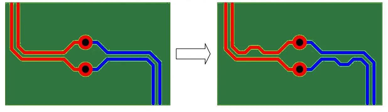
Differential pairs are more sensitive. If both members of the pair are not necked identically, the differential impedance and the common-mode conversion both degrade. Unequal width changes are a frequent source of intra-pair skew and mode conversion that only appears in full-wave simulation or in measured S-parameters.
Current-Carrying Capacity Is Limited by the Narrowest Section
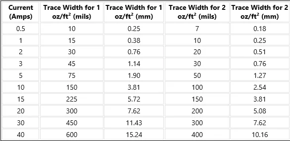
Ampacity and temperature rise are governed by the cross-sectional area of the copper. A wide trace that is necked down for only a few hundred microns still has its current limited by that narrow segment. Heat generated in the neck-down cannot spread effectively into the wider copper if the transition is abrupt, so the local temperature rise is higher than a uniform narrow trace of the same length would produce.
Designers often size the main run for the required current and then forget that the neck-down must also satisfy the same requirement. In power distribution nets or high-current clock lines this oversight creates hot spots that only appear under load. In extreme cases the neck-down becomes a fuse.
IPC-2152 or equivalent charts should be applied to the narrowest width, not to the nominal width of the route. The length of the neck-down still matters for thermal spreading, but the current rating itself is set by the minimum cross-section.
Manufacturing Limits on Variable HDI Trace Width
Every fab has a minimum reliable trace width for a given copper weight and etch process. In HDI that number is frequently 50 µm or 75 µm on outer layers and can be tighter on inner layers with thinner copper. When a design mixes that minimum width with wider sections, the etch compensation and the process window become more difficult to hold.
Narrow sections etch faster relative to their width. Over-etch can open the neck-down or create a high-resistance link. Under-etch leaves residual copper that reduces clearance to adjacent features. The wider portions of the same net do not experience the same percentage change, so the final geometry is no longer a simple scaled version of the artwork.
Yield drops when the neck-down sits at the absolute process floor. A board that would run cleanly with uniform 75 µm traces can show opens or near-opens in the short 50 µm segments. CAM review often flags these transitions because they sit inside the process capability limit rather than comfortably above it.
Signal Integrity Consequences Beyond Simple Impedance
The impedance step is the most obvious effect, but it is not the only one. A neck-down changes the local inductance and capacitance. On a single-ended line this adds a small amount of delay variation. On a differential pair it can unbalance the odd-mode and even-mode velocities if the two members are not treated identically.
When the neck-down occurs near a via or a component pad, the discontinuities interact. The combination of a width change and a via stub or pad capacitance produces a larger reflection than either feature alone. High-speed channels that already operate near their loss or jitter budget have little margin left for these cumulative effects.
Return path discontinuities are also amplified. A narrower trace has a more tightly confined return current. If the reference plane has voids or splits near the neck-down, the return path inductance rises more sharply than it would for a uniform wider trace.
Common Routing Errors That Create Problematic Transitions
The most frequent error is an abrupt step with no transition region. A 100 µm trace that suddenly becomes 50 µm for 200 µm of length and then returns to 100 µm creates two sharp discontinuities. A short taper or a stepped transition reduces the reflection coefficient.
Another common mistake is necking only one member of a differential pair to clear an obstacle. The resulting asymmetry is difficult to compensate and usually shows up as elevated common-mode conversion.
Designers also change width without updating the impedance calculation or the fab's minimum feature note. The net is routed as 50 Ω based on the wide section, yet the narrow section is left uncontrolled. The board is then built to a specification that the physical geometry cannot meet.
Finally, neck-downs are often placed in regions of high current density or high thermal load without checking temperature rise. The narrow section becomes both an electrical and a thermal weak point.
Practical Approaches That Keep Width Changes Under Control
When a width change is unavoidable, keep the narrow section as short as the routing density allows and apply a short taper rather than a hard step. Calculate the impedance for both widths and verify that the discontinuity is acceptable for the edge rate of the signal.
Treat the narrowest width as the governing feature for current capacity and for fab capability. If the neck-down sits at the process minimum, consider whether a slight increase in stack-up density or a different via arrangement can eliminate the need for the change.
For differential pairs, enforce matched geometry through any transition. For power nets, size the neck-down for the full current and accept the density cost, or move the high-current portion to a wider layer or a copper pour.
HDI trace width should be chosen once for the net and held as constant as routing allows. Every intentional change introduces a discontinuity, a current limit, and a manufacturing variable. When the change is required, it should be engineered rather than accepted as an inevitable consequence of density. The boards that perform cleanly are the ones in which width transitions were treated as controlled features, not as afterthoughts forced by the last available routing channel.






