The practical floor for minimum microvia diameter in production HDI is not set by the laser. It is set by copper plating reliability and the process window the fab can actually hold. Most competent HDI lines will quote 75 µm. A few will quote 50–60 µm. Designing to either number without understanding the surrounding constraints is how boards that look fine in layout start failing in reliability testing or, worse, in the field.
Laser drilling can open a 40 µm hole in thin dielectric. That is not the issue. The issue starts the moment the hole has to be metallized, filled, and then survive sequential build-up, reflow, and thermal cycling.
Laser Capability Is Not the Limiting Factor
CO2 lasers still dominate high-volume HDI. Their practical minimum clean diameter on common RCC or thin prepreg is around 70–80 µm. UV lasers can go smaller—50 µm is routine on advanced lines—but the smaller the opening, the more critical the dielectric thickness and the copper thickness on the capture pad become.
A laser will drill what you ask it to drill. The process window collapses when the hole diameter approaches the thickness of the dielectric being removed. At that point the taper changes, the bottom diameter becomes inconsistent, and the subsequent desmear and electroless copper steps see a different surface every panel.
Aspect Ratio Decides Whether the Copper Will Be Reliable
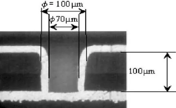
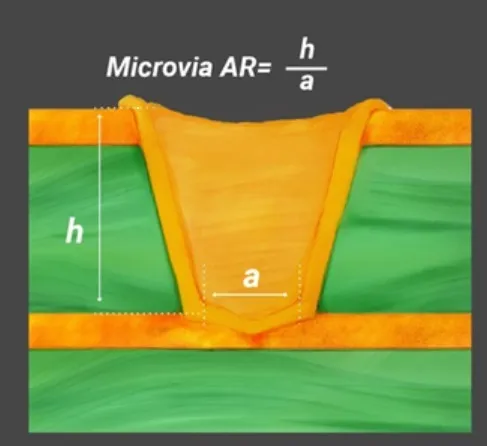
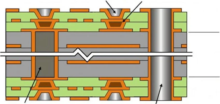
For microvias the aspect ratio that matters is depth divided by the diameter at the narrowest point (usually the bottom). Most production specifications still treat 0.8:1 as the preferred upper limit for reliable filling. 1:1 is accepted on many lines with filled and capped vias. Beyond that the risk rises quickly.
A 75 µm diameter microvia through 60 µm dielectric sits at roughly 0.8:1. Drop the diameter to 50 µm in the same dielectric and you are already at 1.2:1. The electroless copper has to throw into a narrower, deeper cavity. The subsequent electrolytic fill has less room to work. Voids, seams, and thin sidewall copper become statistically more likely.
Stacked microvias make the problem cumulative. Each successive interface inherits any plating deficiency from the via below it. What looks acceptable on a single layer becomes a reliability weak point once three or four microvias are stacked.
What Actually Breaks When Diameter Is Too Small
The failures are rarely dramatic open circuits at electrical test. They are more often intermittent resistance rise after thermal cycling, or cracks that appear only after multiple reflow cycles. Thin copper on the via wall fatigues first. Incomplete fill leaves a stress riser that propagates under CTE mismatch.
On the fab side the yield hit shows up as higher scrap on the plating line and more panels rejected for voids under X-ray or microsection. When the design diameter sits right at the edge of the process capability, small shifts in laser focus, dielectric thickness, or plating bath chemistry move a significant percentage of vias out of the acceptable window.
Capture pad size also shrinks with the via. A 50 µm microvia on a 150 µm pad leaves almost no annular ring once registration, etch, and laser positioning tolerances are stacked. Misregistration then produces a partial via that never makes reliable contact.
Practical Design Limits That Survive Real Production
For most commercial HDI work the safe minimum microvia diameter is still 75 µm when the dielectric is in the 50–70 µm range. That combination keeps aspect ratio under 1:1 with margin and gives the plating process room to operate. Moving to 60 µm is possible on lines that have demonstrated UV laser capability and tight process control, but it should be treated as a special process, not a default rule.
Below 50 µm the conversation changes from "can the fab do it" to "will the product survive its required life." At that size the designer is usually forced into thinner dielectrics, which brings its own impedance and registration problems, or into accepting a higher aspect ratio and the associated reliability risk.
Design rules should include a hard floor that is at least 10–15 µm larger than the absolute minimum the fab claims. That margin absorbs normal variation in dielectric thickness, laser energy, and plating uniformity. It also leaves room for the inevitable process drift that occurs over a long production run.
Safety Margin Is Not Optional
The most common mistake is taking the fab's quoted minimum microvia diameter HDI capability and using it as the design rule. That number is usually the best-case process capability under controlled conditions. Real panels see dielectric thickness variation, copper foil variation, and laser focus drift. Designing to the absolute floor removes all of that margin.
A better approach is to ask the fab for the diameter at which they achieve >95 % first-pass yield on filled microvias across a production lot, not the diameter they can demonstrate on a qualification coupon. Then add another 10 µm. That is the number that belongs in the design rules.
When the stack-up forces smaller vias, the correct response is usually to reduce dielectric thickness rather than to accept a higher aspect ratio. Thinner dielectric restores the aspect ratio and improves plating, provided the impedance targets and registration capability still allow it.
In short, the minimum microvia diameter HDI that is safe for production is the diameter at which the plating process still has room to work, the capture pad still has a usable annular ring after all tolerances, and the aspect ratio stays comfortably under 1:1. Everything smaller is a calculated risk, not a design rule.