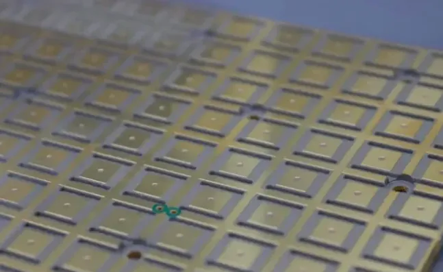
In production we treat fine-pitch HDI BGA solder bridging as a combined fab-to-assembly risk that starts on the CAM screen. For any BGA at 0.5 mm pitch or tighter we force a solder-mask-defined (SMD) pad geometry and lock the mask opening to the copper pad edge with a maximum ±0.025 mm allowance. CAM engineers also reject any remaining mask web thinner than 0.075 mm between adjacent openings because that web cannot survive imaging, development and the subsequent thermal cycles of sequential HDI lamination. Those two rules—SMD definition plus minimum web—are the first line of defense we apply before the panel ever leaves the fab.

Registration stack-up and etch undercut that open the path for bridges
The problem is not theoretical. On a typical 1+N+1 or 2+N+2 HDI stack the solder-mask registration capability is ±0.050 mm to ±0.075 mm after the final press and laser cycles. Copper etching on the outer layers adds another 10–20 µm of undercut per side. When those two tolerances stack, a nominal 0.080 mm mask web can drop below 0.040 mm in local areas. At that thickness the mask lifts or cracks during development, leaving an uncontrolled copper surface between pads. Paste then wets both pads during reflow and forms a continuous solder fillet—the classic HDI BGA solder bridging short.
Material behavior makes it worse. Thin core or resin-coated-copper layers used in HDI expand and contract differently from the thicker outer cores; the differential movement shifts the already-imaged mask relative to the copper. We see this most clearly on panels that have been through three or more sequential lamination steps. The cumulative registration error is why a design that looks clean in the Gerber still produces bridges once it reaches SMT.
Yield loss and rework difficulty when the dam is missing
If the mask web is allowed to disappear, the downstream effect is immediate. Stencil printing deposits paste across the merged copper area; after reflow the excess volume creates bridges that fail both electrical test and X-ray. On 0.4 mm and 0.35 mm pitch packages the bridges are often under the package body, so visual inspection misses them. Rework requires precise hot-air and vacuum tools; even then the pad surface is usually damaged and the board is scrapped. We have measured assembly yield drops of 8–15 % on lots where the fab mask clearance was left uncontrolled. That scrap also pushes delivery dates out by the time needed to rebuild the panel and re-run SMT.
CAM compensation and process limits that keep the dam intact
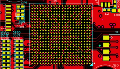
On the CAM side we first convert every fine-pitch BGA to solder-mask-defined geometry. The copper pad is drawn 0.050–0.075 mm larger than the final desired wettable area; the mask opening is then set exactly to the finished pad size. This gives the mask a solid copper ledge to lock onto and produces a consistent dam height of 15–25 µm after cure. For pitches at 0.4 mm we further tighten the mask-to-pad registration compensation to ±0.025 mm and run a dedicated LDI (laser direct imaging) recipe with reduced expansion factors.
We also adjust the outer-layer etch compensation. Instead of the normal 20–25 µm undercut allowance we use a tighter 10–12 µm factor so the finished copper pad stays closer to nominal. After etching, AOI measures the actual pad diameter and mask opening; any site that falls outside the ±0.025 mm window is marked for local repair or panel scrap. These numbers come from our own process capability studies on HDI material sets—FR-4 and high-Tg equivalents—run at the same temperatures the customer will later use in reflow.
Stencil and paste advice is handed to the assembly house as part of the DFM package. We recommend a 0.1 mm or 0.12 mm laser-cut stencil with apertures reduced to 80–90 % of the SMD pad area and Type-4 or Type-5 paste. The reduced volume keeps the solder from overflowing the dam we have already formed. On the fab side we keep copper density balanced within 10 % across the BGA region so panel warpage stays below 0.5 %; excess warpage itself can open the mask registration enough to recreate the bridge path.
Cases where the strict rules can be relaxed
We allow a return to non-solder-mask-defined pads only when the pitch is 0.65 mm or larger and the customer confirms they will use a nitrogen reflow profile with peak temperature held below 245 °C. In those conditions the lower surface tension and reduced paste volume keep bridging risk acceptable even if the mask web is only 0.060 mm. Prototype lots under 20 panels can also run with a 0.050 mm web if the customer accepts 100 % X-ray inspection and is prepared for possible rework. Production volumes stay under the tight SMD rules; the yield cost of a single bridge event outweighs the small design convenience of an NSMD pad.
The same engineering limits apply whether the board is a pure HDI or a hybrid construction. Once the pitch drops below 0.5 mm the mask dam becomes the primary barrier against HDI BGA solder bridging, and the fab must control that dam before the panel is shipped.