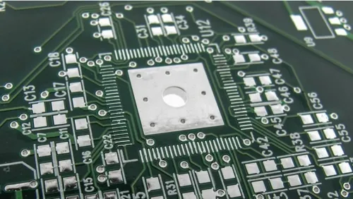
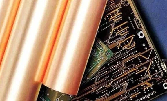
In production, HDI boards that arrive with uneven layer structures are held at CAM until the copper-area ratio between the upper and lower halves sits inside 90–110 % and the core/prepreg distribution is mirrored as closely as the design permits. When the imbalance exceeds that window we either push a redesign request or insert balancing copper and lock a modified press recipe before the first lamination. Most factories treat any sequential-build HDI that lacks this check as a high-risk job and will not release it to the press without documented compensation.
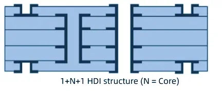
Residual stress that locks in during sequential HDI lamination
The warpage appears because the press cycle freezes differential shrinkage into an already asymmetric structure. Copper expands at roughly 17 ppm/°C while the resin system moves 50–70 ppm/°C in the Z-axis and still higher in-plane once the glass constraint is locally removed. When one side of the HDI carries denser copper or extra sequential build-up layers, that side contracts less during cool-down. The thin dielectric films typical of HDI (50–75 µm) transmit the mismatch more readily than a standard multilayer core, so the panel bows toward the copper-poor face. Larger panel sizes and multiple laser-via layers magnify the effect because the structure has less overall bending stiffness in the early build-up stages.
Copper distribution is the dominant driver. A layer that is 70 % copper next to a layer that is only 20 % copper creates a local CTE gradient that the prepreg cannot fully absorb. Material CTE differences between cores and prepregs of different glass styles add a second gradient. Even when the designer keeps total layer count even, an uneven copper map or mismatched prepreg construction still produces measurable residual stress after the final cool-down. In practice we see the largest HDI PCB warpage on builds where the outer sequential layers are heavily loaded with microvias while the opposite side remains nearly empty.
Yield loss and downstream registration failures when the imbalance is ignored
Uncontrolled HDI PCB warpage routinely pushes finished boards past the 0.75 % bow-and-twist limit in IPC-6012. Once the panel is out of tolerance, mechanical drilling and routing show registration offsets of 25–50 µm, enough to eat annular ring on 0.2 mm vias. Solder-mask alignment drifts, leaving exposed copper or reduced mask dams between fine-pitch pads. At assembly the same boards produce open BGA joints, tombstoning on 0201 parts, and occasional conveyor jams on the pick-and-place line. Scrap rates on high-density sequential HDI jobs climb from the normal 1–2 % into the 5–8 % range when warpage is left unaddressed. Each extra re-lamination or mechanical flattening cycle also adds two to three days to the ship date.
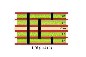
CAM copper balancing and process compensation used on the production floor
Factories close the gap with a combination of design-rule enforcement and process-side compensation. On the CAM station we run automated copper-area calculations for every layer pair and insert non-functional pours or cross-hatch patterns wherever the local density falls below the opposite side by more than 10 %. Stackup is forced toward mirror symmetry by matching core thicknesses and prepreg glass styles on both sides of the centerline; when a design insists on extra microvia layers on one face we still keep the dielectric thickness and resin content as balanced as possible. During lamination the cool-down rate is held under 3 °C/min and steel caul plates maintain uniform pressure across the panel. After each sequential build-up a multi-point laser or feeler-gauge check quantifies residual bow; any panel that exceeds 0.5 % receives a 120–150 °C stress-relief bake for two to four hours before the next laser process. On the most critical HDI lots some lines also use constrained fixtures that lock the panel flat through the entire cool-down window.
These steps are used because they attack the root cause—residual stress—rather than trying to flatten a finished board after the fact. Copper balancing reduces the driving force; controlled cooling and post-bake release the stress that has already formed; the measurement loop catches any remaining deviation before the next process locks it in permanently. The net result is that HDI PCB warpage stays inside the specification even when the original design was only marginally balanced.
Cases where an asymmetric HDI stackup is still released
Exceptions are granted when the electrical or density requirements genuinely prevent symmetry—most often when one side needs extra microvia layers for high-pin-count BGA breakout while the opposite side stays simple. In those situations we accept a relaxed bow-and-twist limit (commonly 1.0–1.5 %) after the customer signs a deviation, and we compensate with thicker outer cores or higher-Tg materials that raise the overall stiffness. The trade-off is a modest yield reduction and the need for assembly fixtures that hold the board flat during reflow. Rigid-flex HDI hybrids fall into the same category because the flex section forces asymmetry by construction; those jobs are released only after the rigid zones have been copper-balanced as far as the design allows and the customer has accepted the residual warpage risk.