In production we treat sheet metal enclosure thermal management as a combined PCB-to-chassis heat path problem. When a design lands on the CAM desk we first calculate the total power dissipation from the board, map the primary heat sources, then check whether the copper planes, component placement and enclosure contact points can move that heat into the metal walls without creating local hot spots. If the numbers do not close we flag the file and ask for either more copper, thermal vias, or a change in the enclosure interface before the panel is released.
Where the heat path breaks during real panel builds
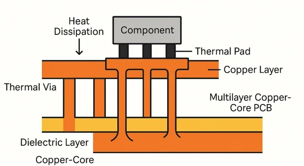
Most failures start on the board itself. The sheet metal is only as effective as the thermal resistance between the die and the chassis. In practice we see copper planes that stop short of the mounting holes, thermal vias that are plugged solid by solder mask, or high-power parts sitting on the opposite side of the board from the enclosure contact surface. Once the board is fabricated those gaps cannot be fixed without a respin. Material choice on the enclosure side compounds the issue: cold-rolled steel conducts roughly half as well as aluminium of the same thickness, and any powder-coat or anodise layer adds another thermal barrier that designers often ignore until the first thermal chamber run.
Ventilation holes are another common source of trouble. We routinely receive drawings with louvers placed for cosmetic reasons rather than air-flow direction. In a sealed or semi-sealed sheet metal box natural convection only works if the inlet and outlet form a proper chimney path. When the holes are staggered or partially blocked by internal brackets the air simply stagnates and the PCB temperature rises 15–25 °C above the predicted value.
What shows up on the production floor when the path is ignored
Boards that leave the fab looking perfect still fail later. The first symptom is usually solder-joint fatigue on power components after a few hundred thermal cycles. The second is field returns with scorched FR-4 around high-current traces. On the assembly line we also see higher scrap rates during functional test because the unit overheats inside the closed enclosure long before the specified ambient limit is reached. When the enclosure is already powder-coated and the PCB is already populated, the only recovery options are adding external heat sinks, cutting extra vents, or applying thermal pads—none of which are free and all of which delay shipment.
From a yield standpoint we track these failures as "thermal DFM escapes." They rarely appear on the bare-board electrical test, so they slip past final inspection and become customer problems. That is why we push the conversation upstream during the initial DFM review rather than after the first article is built.
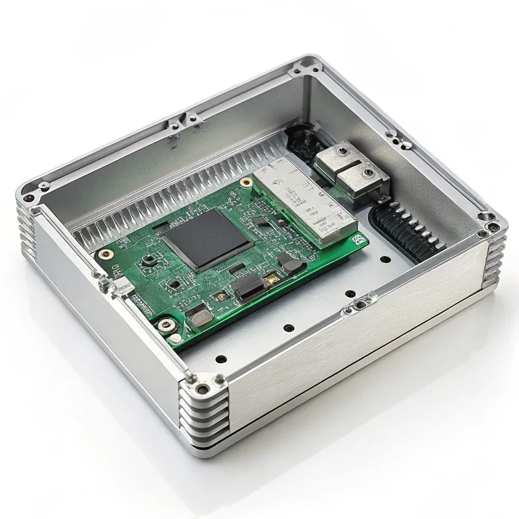
How the factory actually closes the thermal loop
On the CAM side the first step is a simple heat-path checklist. We require at least 70 % copper coverage under any power device that is expected to dump heat into the chassis. Thermal vias under those pads are kept open (no solder-mask tenting) and are sized 0.3 mm finished hole so they fill with solder and form continuous copper columns. If the enclosure has a flat mounting boss we ask for a matching copper pour on the PCB bottom layer with a clearance of 0.2 mm around the screw hole so the board can sit flush.
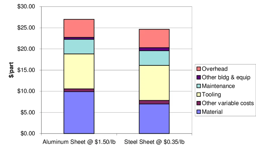
For the enclosure itself we prefer 1.5–2.0 mm aluminium over steel whenever the weight budget allows. The conductivity difference is large enough that we can often drop from forced-air to natural convection. When steel is mandatory we recommend a bare metal contact zone under the high-power area—no paint, no anodise—and a thin thermal interface material rated for the expected surface pressure. Ventilation holes are sized and located by the same rule we use for internal airflow: inlet area at least equal to the total exhaust area, and the path must run past the hottest components rather than around them.
Natural cooling versus active cooling is decided by the power density and the enclosure volume. Below roughly 0.1 W/cm³ we stay with natural convection and rely on the sheet metal surface area. Above that threshold we either add a small fan with a defined airflow path or increase the external heat-sink area. The PCB layout is adjusted accordingly: high-power parts move closer to the fan intake or to the external heat-sink mounting points so the copper planes can short-circuit the heat to the metal rather than letting it spread across the board.
During panel design we also leave clear zones around the board edges that will contact the chassis. Any solder-mask or legend that would sit under a thermal pad is removed so the copper can touch the interface material directly. These rules are applied automatically in our CAM scripts once the power budget is entered; the designer only needs to confirm the numbers.

When the strict rules can be relaxed
Low-power designs under 5 W total dissipation can usually skip the full thermal-via array and still meet ambient ratings inside a moderately sized aluminium box. The same applies to boards that spend most of their life in free air rather than sealed enclosures. In those cases we still keep the copper pour continuous under the main heat sources, but we drop the via density and allow solder-mask over the secondary thermal paths. The trade-off is clear: the design is cheaper and faster to fabricate, yet it leaves less margin if the enclosure later changes or the ambient temperature rises. We document the assumption in the DFM notes so the next revision does not inherit an optimistic thermal model.
The practical limit remains the same whether the cooling is natural or forced: the PCB copper and the sheet metal must form a continuous, low-resistance path. Everything else—vent size, material grade, fan choice—is secondary to that basic requirement. When the path is intact the enclosure becomes an asset rather than a thermal trap.