










PCB Fiducial Mark: SMT Alignment & DFM Rules
What This Video Covers
This video isolates a feature most engineers walk past on a panel rail: the small exposed copper circle used as a PCB fiducial mark. That mark is not artwork. It is the optical datum that stencil printers, pick-and-place machines, SPI, and AOI use to lock X/Y position, rotation, and—when a third mark is present—scale or warp. The clip distinguishes global marks on the board, panel marks on the process rail, and local marks next to fine-pitch packages, then states the practical layout rules: keep marks far apart, leave a clean keep-out around each target, use a 1–3 mm copper diameter with 1 mm preferred, fully open the solder mask, and respect the IPC edge offset of 4.75 mm plus the required fiducial clearance. Double-sided SMT may need the same targets on both sides. Those rules matter on HDI PCB layouts, 4 layer PCB control boards, and any job moving from PCB prototype into turnkey PCB assembly. Watch the short, then apply the same checklist before you request an SMT assembly quote.
Key Highlights
- Fiducials are global, panel, or local: board-level references, panel-rail references, and local marks that lock fine-pitch packages such as BGA, QFN, and QFP.
- Two marks correct position and rotation; a third mark lets the vision system compensate for stretch, shrink, or panel distortion.
- Preferred copper diameter is 1 mm (range 1–3 mm), solder mask must fully expose the copper, and IPC requires 4.75 mm plus the fiducial clearance from the board or panel edge.
How Fiducial Marks Guide SMT Machines
A fiducial mark is a high-contrast optical target etched in the same copper artwork as the component pads. Typical construction is a solid filled copper circle, a solder-mask opening large enough that no resist covers the copper or the keep-out ring, and no silkscreen, copper pour, or text inside that ring. Because the mark is photodefined with the circuit, its position relative to every footprint is known to the same accuracy as the pads themselves. That is why a drilled hole, a mounting hole, or a silkscreen dot is a poor substitute: hole location and ink print are not registered to the copper with the same process.
When a panel or single board enters a stencil printer or pick-and-place machine, the camera searches for these circles, calculates the centroid of each, and builds a coordinate frame. Two marks give translation and rotation. A third non-collinear mark adds scale and residual warp, which is common after lamination, routing, or moisture bake on FR4 PCB and multilayer stacks. The same frame is reused by solder-paste inspection and AOI, so a missing or unreadable fiducial does not stay a "placement" problem—it becomes a paste-offset, tombstone, and inspection-false-call problem on the same lot.
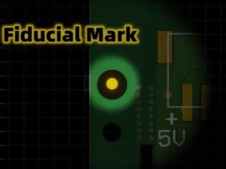
Factory practice is blunt: if the camera cannot lock two clean marks in the first scan, the line stops or the operator overrides with a slower, less repeatable teach. That is expensive on PCB mass production and still wasteful on a first article. Design the marks so the first scan succeeds.
Global, Panel, and Local Fiducials Compared
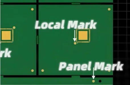
Not every copper circle on the panel does the same job. Mixing the three types—or putting all of them on a rail that will be broken off—is a frequent CAM finding.
Global fiducials sit on the finished board, usually near opposite corners and as far apart as the outline allows. They establish the board's own coordinate system after the panel is located, and they remain after depanel so rework, selective solder, and field service fixtures can still register.
Panel fiducials sit on the process rail or breakaway frame. They locate the entire array for stencil print and first-side placement. Rails exist partly so tooling holes and optical points can live off the product. If the only marks on the job are on a V-cut rail, they disappear after depanel and the assembled unit has no remaining optical datum.
Local fiducials sit next to a fine-pitch land pattern. They shrink the vision field so a 0.4 mm or 0.5 mm BGA, a tight QFN, or a fine-pitch connector is placed against a nearby datum instead of a corner several tens of millimeters away. On high-density consumer electronics PCB and automotive PCB layouts, local marks often decide whether first-pass yield holds when copper stretch is a few tens of microns.
| Fiducial type | Typical location | Primary job on the line | Recommended count |
|---|---|---|---|
| Global (board) | Opposite corners of the finished PCB, far apart | Board X/Y, rotation; remaining datum after depanel | 2 minimum, 3 preferred (non-collinear) |
| Panel (rail) | Process edge / tooling rail, off the product outline | Array alignment for stencil print and first-side SMT | 3–4 per panel, kept off V-cut paths |
| Local (component) | Adjacent to BGA, QFN, QFP, fine-pitch connectors | Component-level correction when global span is too large | 2 per critical package, or shared between adjacent packages |
Why Two Marks Are the Minimum and Three Are Better
Two marks on a long baseline correct offset and theta. They cannot separate uniform stretch from a camera calibration error, and they cannot describe a bow between the two points. A third mark, placed so the three points form a large triangle rather than a line, lets the machine apply a simple affine correction. That third mark is cheap copper. Skipping it on a large 6 layer PCB or a panel with mixed copper density is how "the placement file was perfect" still yields a systematic 50–80 µm shift in the center of the array.
Place marks far apart. Two 1 mm circles 15 mm from each other on the same corner give a noisy rotation estimate. The same two circles on opposite corners of a 100 mm board give a usable theta. Keep the keep-out around each mark empty: no traces, no vias, no legend, no mask sliver. Vision algorithms need a clean ring of laminate contrast, not a copper hatch under the opening.
Fiducial Size, Solder Mask Opening, and IPC Edge Clearance
IPC land-pattern practice (IPC-7351 family) treats the optimum fiducial as a solid filled circle. Diameter range is 1.0 mm to 3.0 mm; 1.0 mm is the preferred value used by most SMT cameras and by most AIVON DFA reviews. Marks on the same board should not differ by more than 25 µm. Mixing a 1 mm global with a 2.5 mm "logo-sized" local mark forces the vision recipe to hunt two geometries and is a common first-article delay.
Solder mask must fully expose the copper and the clearance zone. A mask that kisses the copper edge breaks the circular centroid and drops contrast, especially on dark soldermask over oxidized copper. Preferred construction is:
- Copper diameter: 1.0 mm (acceptable 1.0–3.0 mm)
- Mask opening: concentric, radius at least 2× the copper radius (so a 1.0 mm copper mark gets at least a 2.0 mm keep-out diameter; many assemblers prefer ~3.0 mm)
- Surface: flat copper or a thin, consistent finish (ENIG is easy to image; heavy HASL can dome and scatter)
- Flatness target: within about 15 µm so the camera does not see a solder bump as an offset centroid
Edge clearance is the rule that conflicts with cramped outlines. IPC specifies that the fiducial must sit no closer to the board or panel edge than 4.75 mm plus the required fiducial clearance. The 4.75 mm term is the SMEMA transport / clamp zone. A 1 mm mark with a 1 mm radial keep-out therefore wants its copper edge well inside the clamp-safe area—not on the routed outline and not on a V-score. If the product outline cannot accept that offset, put the panel marks on a 3–5 mm process rail and keep at least two global marks on the finished board so assembly and later inspection still have a datum.
| Parameter | Practical target | Why the line cares |
|---|---|---|
| Copper diameter | 1.0 mm preferred (1.0–3.0 mm allowed) | Matches most P&P / printer camera recipes |
| Size match on one board | ≤ 25 µm variation | One vision model, no mixed-target hunting |
| Mask / feature keep-out | ≥ 2× copper radius, concentric | Clean contrast ring; no mask sliver on the centroid |
| Edge offset | 4.75 mm + fiducial clearance (IPC) | Clears conveyor clamps and router / V-cut damage |
| Double-sided SMT | Repeat marks on both assembled sides | Second-side print and place cannot use first-side copper |
| Finish | Flat ENIG or controlled copper; avoid thick HASL domes | Stable reflectivity and centroid |
For double-sided assembly, copy the scheme onto the second side. A board that only has first-side fiducials will print and place the second side against tooling holes or against a taught corner—both worse than copper datums registered to the pads. Flex and rigid-flex PCB jobs add another constraint: do not put the only optical points on a polyimide zone that wrinkles in the fixture. Keep them on the rigid region or on a stiffener-backed rail.
If you are also ordering a SMT stencil, the stencil needs matching half-etched or cut fiducials so print registration uses the same datum the placement machine will use. A perfect board fiducial with no stencil fiducial still prints paste in the wrong frame.
Common Fiducial DFM Failures That Stop SMT Lines
The failures that show up in CAM and on the first SMT shift are repetitive.
Mask covering the copper. A soldermask-defined "almost circle" is not a fiducial. The camera either fails to find it or locks on the mask opening instead of the copper, which is offset by the mask registration tolerance—often 50–75 µm, enough to walk a 0.4 mm BGA off pad.
Marks on the V-cut. A panel fiducial drawn on the score line is gone after depanel and may already be half-destroyed when the printer camera looks at it. Keep optical points off the machined path.
All marks on a disposable rail, none on the board. Fabrication can register the panel. After the rail is broken off, the assembled product has no global datum for second-side SMT, AOI, or fixture load. Put panel marks on the rail and global marks on the product.
Marks too close to the edge. Clamps, conveyor belts, and the router spoil the contrast ring. IPC's 4.75 mm plus clearance exists because SMEMA handlers occupy that strip. If the outline is too tight, add a rail rather than crowding the mark into the clamp zone.
Inconsistent size or non-circular artwork. Crosses and squares etch with rounded corners and a wandering centroid. Circles survive etch variation. Keep every mark on the job the same diameter.
No local marks on a large fine-pitch device. Global marks at the corners of a 150 mm industrial control PCB cannot correct local copper stretch next to a 0.4 mm BGA. Two local marks on the diagonal of that package are cheaper than a scrap array.
Oxidized or bumped surfaces. Bare copper left open for weeks, or HASL that leaves a solder mound, changes reflectivity and centroid. Specify a finish the assembler has already qualified for vision, and keep the fiducial out of the HASL "thick deposit" zones if HASL is mandatory.
Treat fiducials as part of the DFA package with panel rails, tooling holes, and stencil datums—not as leftover copper. When those four items agree, PCB assembly first-pass yield is limited by paste and parts, not by a 1 mm circle the camera never found.
FAQ
Q1: How many fiducial marks does an SMT job need on a single board versus a panel?
A1: A single board should carry at least two global marks on a long baseline; three non-collinear marks are the production default because they correct stretch and warp. A panel should add three to four panel marks on the rails for print and first-side place. Fine-pitch BGAs, QFNs, and connectors still need their own local pair. Do not count rail-only marks as the board’s remaining datum after depanel.
Q2: What happens if solder mask partially covers the fiducial?
A2: The vision system either misses the target or locks on the mask opening, which is offset by mask registration. That offset transfers into paste and placement. Fully open the mask over the copper and the keep-out ring. If CAM flags mask on the mark, treat it as a stop-ship DFM item, not a cosmetic note.
Q3: Do double-sided SMT boards need fiducials on both sides?
A3: Yes, if both sides are printed and placed. Second-side equipment cannot see first-side copper. Mirror the global scheme onto the second side, and add local marks next to second-side fine-pitch parts. Odd-form or wave-only second sides can sometimes share tooling holes, but automated SMT on side two should not rely on that.
Q4: Can local fiducials be skipped on a 0.4 mm pitch BGA if three global marks already exist?
A4: Not on a large board or a panel with uneven copper. Global marks correct the whole image; they do not remove local laminate movement across a 20–30 mm BGA. Two local marks on the package diagonal are the low-cost insurance. Confirm with the assembler before deleting them to recover routing space.
Q5: Does surface finish change whether the fiducial is readable?
A5: Yes. Flat ENIG or controlled copper gives stable contrast. Thick HASL can dome the pad and scatter the camera. OSP can oxidize if the board sits. Specify one diameter, one finish behavior, and a mask opening that does not leave a resist sliver. If HASL is required, keep fiducials out of heavy-deposit regions and verify first-article vision lock before releasing the stencil.
This is a PCB edge rail.
But look closer.
That tiny copper circle?
That's a fiducial mark.
It helps SMT machines locate the board and place components accurately.
Fiducials can be global, panel, or local.
Global marks reference the board, panel marks reference the panel, and local marks align fine-pitch components.
For board alignment, two marks correct position and rotation.
A third can help compensate for distortion.
Place them far apart, with a clean area around each mark.
A typical fiducial is 1 to 3 millimeters in diameter, with 1 millimeter preferred.
The solder mask should fully expose it.
IPC specifies 4.75 millimeters plus the required fiducial clearance from the board edge.
For double-sided assembly, fiducials may be needed on both sides.
Small mark, big role in SMT.





