In wireless communication circuit design, the mixed behavior of baseband and RF makes electromagnetic compatibility (EMC) one of the hardest constraints. If EMC is not met, the product can fail radiated-emission limits, lock up under ESD, or drop communication, all of which reduce reliability. The following 15 PCB layout methods are drawn from circuit principles and practical work on controlling electromagnetic interference.
The Root of EMC Problems
EMC is the ability of an electronic system to keep acceptable performance in its intended electromagnetic environment without injecting large amounts of interference into that environment. It has two main sides: radiated emissions and immunity. Common EMC failures—system lock-up, signal distortion, lost communication—trace back to improper radiation and coupling of electromagnetic fields.
In principle, a time-varying current in a closed loop that is terminated in a load produces a fluctuating magnetic field. If the near field and far field of that magnetic field cannot move together, a kink forms and electromagnetic waves are radiated. A digital square wave is made of a series of harmonics of decreasing amplitude. The fluctuating magnetic fields from those current harmonics travel by coupling or radiation and are a primary source of electromagnetic emission. Loops in the PCB routing, and a poor power and ground arrangement, further amplify the radiation and create a loop-antenna effect.
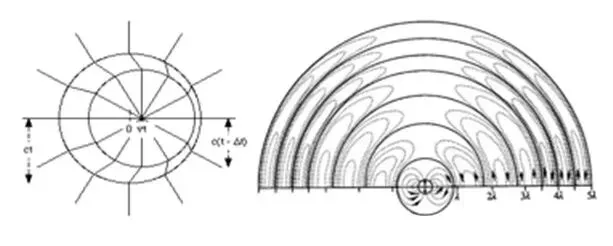
Figure 1 | Kink and radiation mechanism
In general, a differential signal formed by two parallel conductors that are short compared with a wavelength is unlikely to produce a kink. Once the conductors open at an angle, the fields no longer stay coordinated, near-field and far-field regions form, a kink appears, and the structure behaves as an antenna. That is also the operating principle of a wireless antenna.
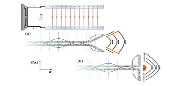
Figure 2 | Formation of the far field
The baseband square wave in a digital circuit contains a large set of harmonics. The fluctuating magnetic field from those current harmonics couples or radiates into the rest of the circuit and is an important cause of EMC problems.
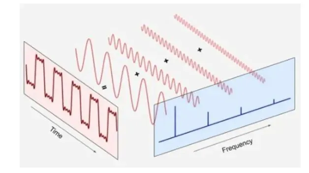
Figure 3 | Harmonic content of a digital signal
If power, signal, and ground are routed as separate paths on the PCB, and a loop length approaches the wavelength of a high-frequency component, the structure readily becomes a loop antenna. High-frequency harmonics then couple in through the electromagnetic field and make the EMC problem worse.
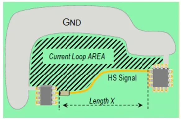
Figure 4 | Loop antenna created by PCB routing
15 Practical PCB Layout Techniques for EMC
Routing Basics: Avoid Creating a Radiating Antenna
-
Control signal loop area
If a high-frequency signal loop approaches a harmonic wavelength, it readily becomes a loop antenna. Keep the loop area as small as possible in the layout to reduce radiated emissions.
-
Prefer differential pairs
A differential signal on two parallel conductors keeps the fields coordinated, reduces kink formation, and lowers the radiation risk.
-
Length-match differential pairs tightly
Closed circuits that include differential signals must be implemented with equal-length traces. Also provide proper power matching and ground fencing so the transmission behavior stays stable and the pair is less disturbed by external fields.
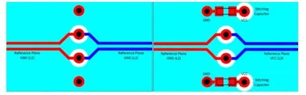
Figure 5 | Equal-length principle for a differential circuit
Power and Ground: The Core of EMC Control
-
Keep power and ground close together
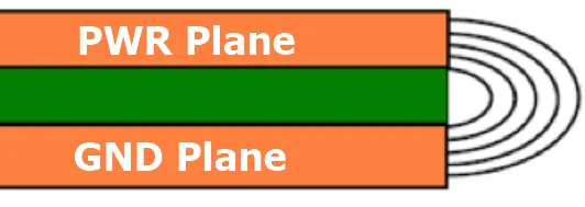
Do not route power and signal traces far from ground. The routing structure of a conventional single-sided board produces an antenna effect at high communication rates. Place power next to ground. A small closed loop on the return path, as in the right-hand arrangement, can cut radiation and coupling substantially.
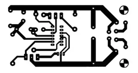
Figure 6 | Conventional single-sided placement and routing
-
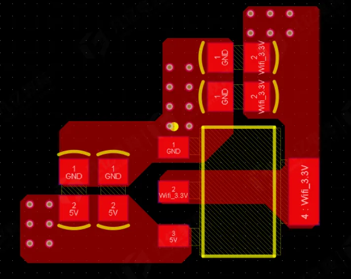
Place the main-chip supply locally
The supply for the main IC should follow the small power-to-ground closed-loop rule. That reduces radiation from the loop and also reduces the chance that other fields will couple into it.
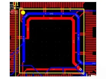
Figure 7 | Recommended main-chip power placement
-
Place capacitors by the reservoir rule
Treat each capacitor as a reservoir. Upstream stored energy must be able to supply the downstream demand. If the current is interrupted, a strong electromagnetic disturbance is launched.
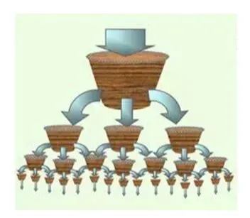
Figure 8 | Reservoir model for current supply
-
Separate the loops in a DC-DC converter
A DC-DC converter contains a high-frequency AC chopping loop, a DC input loop, and an output loop. The AC loop chops a high-speed PWM waveform and readily produces electromagnetic cutting. Keep the three loops apart in the layout so their radiation does not add.
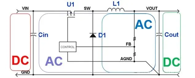
Figure 9 | DC-DC power topology
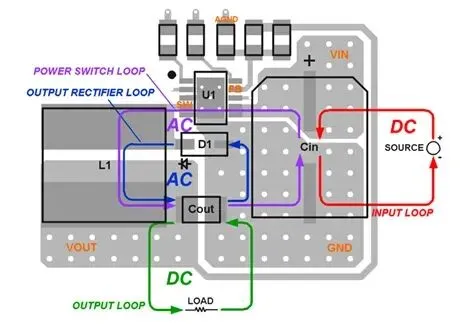
Figure 10 | DC-DC placement and routing recommendations
Circuit Structure: Build a Transmission Path That Rejects Interference
-
Use a fully enclosed coaxial path where appropriate
On a transmission path, a coaxial structure confines the electromagnetic field inside the cable. That cuts radiation loss and external pickup and addresses EMC problems in high-speed signal transmission.
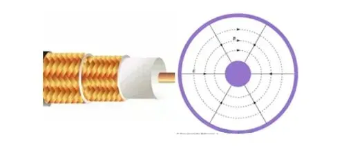
Figure 11 | Coaxial coupled electromagnetic field
-
Match the transmission-line impedance
At high frequency, capacitive and inductive loads, not only resistive loads, produce reflected signals. Insert a passive network between the source and the load so the load impedance matches the source impedance and transmission-line loss from reflection is reduced.
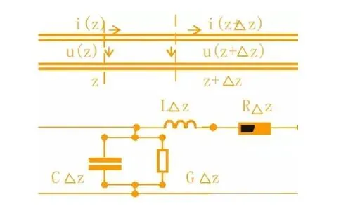
Figure 12 | Synchronous model
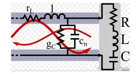
Figure 13 | Connector principle
-
Keep the circuit closed
In a closed circuit, DC current does not produce an alternating magnetic field, while AC current produces a coil-like field. Implement the circuit as a true closed path. A closed loop is difficult for an external field to penetrate, which raises immunity.
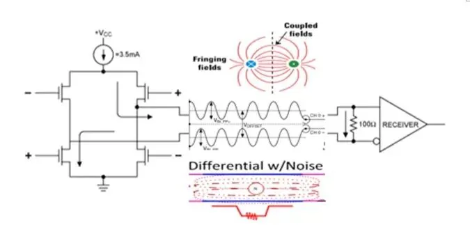
Figure 14 | Differential circuit model
Detail Measures: Reduce EMC Risk Across the Board
-
Do not run signal traces parallel to power traces
Parallel runs couple readily. Where traces must cross, keep a safe spacing so the coupled energy stays down.
-
Keep sensitive parts away from radiators
Keep receivers and other sensitive parts away from oscillators, power devices, and other high-frequency sources. That reduces faults driven by radiated susceptibility, such as abnormal signal output or a system reset.
-
Provide a continuous reference plane
Use a continuous GND plane (for example, GND on L2 and L3 in the stack-up discussed here) as the signal return path. That reduces ground bounce and keeps the noise from degrading circuit performance.
-
Add filter capacitors at the supply
Place filter capacitors at the power input and output to suppress high-frequency noise on the supply rails and keep that noise from spreading through the system.
-
Add ESD protection at interfaces
I/O connectors are exposed to electrostatic discharge. Add ESD protection devices so a discharge does not lock up the system, force a reset, or fault a display panel.
The Governing Logic in Practice
EMC work in PCB layout is a matter of controlling how electromagnetic fields are generated and how they propagate. Tight power-to-ground pairing (the right-hand arrangement in the single-sided example and the main-chip supply loop) reduces loop radiation. Minimum loop area (avoiding the loop antenna in Figure 4) keeps the board from becoming an antenna. Accurate impedance matching (the connector arrangement in Figure 13) reduces interference from signal reflection.
Those three rules run through all of the techniques above. In a real design, keep current continuous with the reservoir rule (Figure 8), cut radiation with differential routing (Figures 2 and 5) and coaxial structures (Figure 11), and separate DC-DC loops (Figure 10) so electromagnetic cutting does not stack. That combination addresses excess radiation, ESD failures, and weak immunity.
Summary
EMC problems are tractable if the field-propagation behavior described above is applied in four places: routing, power and ground, structure, and detail practices. Used at layout time, the 15 techniques can raise system electromagnetic compatibility before hardware exists.
Prevention in the layout is more efficient and less costly than fixing EMC after the board is built.