A wall outlet supplies 220 V AC. Phones, PCs, and routers use 5 V or 3.3 V DC. The conversion between those two domains is AC-DC. The grid also does not distribute low-voltage DC. The sections below cover why AC-DC exists, the two conversion methods, a complete circuit, and the PCB details that usually decide whether the supply is stable.
1. Why AC Must Be Converted to DC
1. Most electronics run on DC
Phones, microcontrollers, ICs, and sensors almost all run on low-voltage DC, most often 5 V or 3.3 V. AC polarity keeps reversing. A chip cannot use that waveform. Without DC conversion it will not start.
2. The grid must transmit AC
Generating stations are often far from the load. For long-distance transmission:
- AC advantage: high voltage and low current, so transmission loss stays low.
- DC drawback in this comparison: voltage step-up is harder, loss is higher, and cost is higher. The grid therefore transmits high-voltage AC, steps it down to 220 V AC at the customer, and lets each product convert to DC.
The grid uses AC to move energy efficiently. The product uses DC to operate safely. AC-DC is the conversion between those two systems.
2. Two AC-to-DC Paths
Two mainstream methods exist. Principle, structure, and trade-offs are different.
Method 1: Line-frequency transformer conversion
Three-step flow:
- A line-frequency transformer first takes high-voltage AC to low-voltage AC, matched to 50/60 Hz mains.
- A rectifier takes low-voltage AC to pulsating DC.
- Capacitor filtering reduces ripple and produces a relatively steady DC.
Characteristics:
- Simple circuit, lower interference, lower cost.
- Large volume, heavy, hotter, lower efficiency. Suited to low-power, low-requirement, low-cost designs.
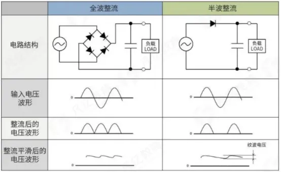
Figure 1 | Rectifier methods
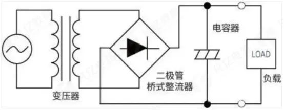
Figure 2 | Transformer AC-DC block diagram
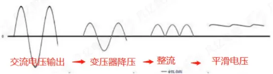
Figure 3 | Waveforms in the transformer method
Method 2: Switch-mode conversion
Chargers, adapters, and most switch-mode supplies use this path. Six conversion steps:
- Bridge rectifier: AC to high-voltage DC.
- Input capacitor: smooths the voltage.
- Switching transistor chopping: turns the DC into a high-frequency pulse.
- High-frequency transformer: steps down and isolates, producing a square wave.
- Output diode: half-wave rectification.
- Output capacitor: filters again and produces regulated DC.
Characteristics:
- Smaller, lighter, higher efficiency.
- More complex circuit, more interference, harder EMC. Suited to phone chargers, PC supplies, industrial supplies, and most other products.
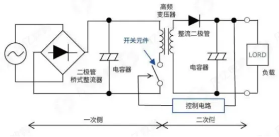
Figure 4 | Switch-mode AC-DC block diagram
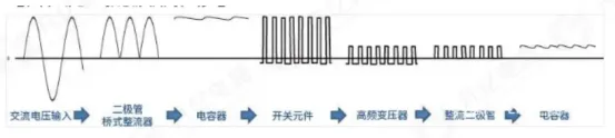
Figure 5 | Waveforms in the switch-mode method
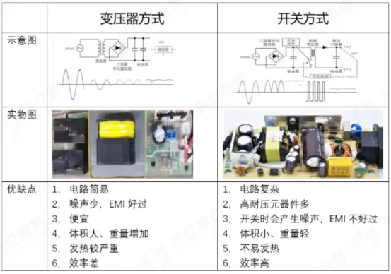
Figure 6 | Advantages and disadvantages of the two methods
3. A Complete AC-DC Circuit Is More Than Conversion
Conversion alone is not a finished supply. A qualified AC-DC power stage usually includes six blocks:
- Input filter: removes high-frequency noise and interference and protects the downstream stage.
- Rectifier bridge: four diodes take AC to pulsating DC.
- Filter network: capacitors and/or inductors reduce ripple.
- Regulation: feedback holds the output voltage.
- Protection: overcurrent, overvoltage, and short-circuit protection.
- Control: the IC plus feedback sets the timing of the converter.
4. Example Circuit: HFC0500
The flow on a common HFC0500 design is:
- Fuse + common-mode inductor + X capacitor: overcurrent protection and interference filtering (Y capacitors filter common mode).
- Rectifier bridge + bulk capacitor: AC to smoothed high-voltage DC.
- RCD snubber: protects the switch from peak voltage.
- HFC0500 pin 5 drive output: switches the transistor at high frequency.
- High-frequency transformer T1: step-down plus galvanic isolation.
- Output diode + capacitor: rectify and filter to the target voltage.
- Optocoupler feedback: isolated sensing for regulation.
5. Five AC-DC PCB Rules
AC-DC combines high voltage and high frequency. A layout error can produce interference, heat, or a destructive fault.
1. Keep the three loops as small as possible
Immunity follows loop area. Smaller is better:
- Input loop: C1 → T1 → Q1 → R11/12/13 → C1
- Auxiliary-winding loop: T1 → D4 → R4 → C3 → T1
- Output loop: T1 → D6 → C10 → T1
A smaller loop radiates less and rejects more interference.
2. Split GND and join it at one point
Input ground and control ground meet at a single point, only at C1, so a ground loop does not form.
3. Isolate high-frequency noise
- Connect the Q1 heatsink to main GND.
- Cut the board outline around the high-frequency switching region to isolate the noise physically.
4. Treat the feedback net as critical
- Keep power traces and the feedback trace fully separated.
- Keep the feedback trace as short as possible and away from noise sources.
5. Keep the optocoupler isolated
Cut the board outline between the optocoupler pads so primary and secondary stay electrically isolated. That supports safety spacing and immunity.
6. Summary
AC-DC looks dense until it is split into three layers:
- Why convert: the grid uses AC; the load uses DC.
- How to convert: transformer or switch-mode. Switch-mode is the mainstream path.
- How to finish it: a complete circuit, protection, and PCB detail.
Those three layers are enough to review both a first AC-DC design and a later respin.