










This Q&A compiles concise, practical tips for common workflows and troubleshooting in Altium Designer across several versions. Topics include rule export, single-sided PCB setup, via stitching patterns, test point placement, Gerber output layers, component designators, and typical installation or stability issues.
1. Preferences cannot be opened in AD09
In some AD09 builds, the Preferences dialog may not open due to a software bug. Try using the TP shortcut to invoke the Preferences panel directly. If the dialog still fails to open, save and restart the application and reattempt via the shortcut.
2. How to import and export design rules
Use the DR shortcut to open the Rules Manager. In the left-side tree, right-click to access the Export Rule function. Select all rules to export them into a rules file for reuse across projects. To reuse rules in another project, access the same menu and import the saved rules file.
Exporting rules is useful when you want to standardize constraints such as clearance, width, via styles, differential pair settings, polygon connect modes, and high-speed rules across multiple projects or teams. Keeping a versioned rules file helps ensure designs follow consistent manufacturing and SI/PI constraints, especially when switching board houses or stackups.
3. AD17 reports a problematic installation path
If the installer repeatedly reports a path error even when using the default path, the package may be corrupted or incomplete. Download a fresh, verified installer and perform a clean installation. Avoid partial updates or mixed-version component packages.
4. How to create a single-sided carbon-ink or single-layer PCB
For a single-sided board, confine all routing and copper features to one layer. Do not place vias, and ensure no copper, pads, or mechanical features that imply a second copper layer are present. In the layer stack, maintain only one active copper layer for routing, with associated solder mask and silkscreen as needed.
In practical terms:
- Route only on the designated top or bottom copper layer.
- Avoid through-hole vias or microvias, as these imply multilayer connectivity.
- Ensure the opposite copper layer remains empty, including polygons and pours.
- For carbon-ink applications, coordinate with the fabricator on the dedicated carbon-ink layer conventions and any special clearances, plating, or curing requirements.
This approach keeps the design DFM-friendly for single-sided processing and avoids adding unintended fabrication steps.
5. Placing regularly spaced vias and low-voltage safety clearance
When stitching ground planes or building via fences, a practical approach is to place stitching vias at a regular pitch, for example every 150 mil, depending on EMI targets and board constraints. In Altium Designer versions 14 and above, dedicated via stitching features can automate patterned via insertion along board edges or polygon boundaries.
For low-voltage circuits, maintain appropriate electrical safety clearance according to your system voltage, pollution category, and manufacturing capability. Keep clearance and creepage rules aligned with your fabricator's process and the applicable safety standards for your product. Implement clearance constraints in the Rules Manager so violations are flagged during routing and polygon repours.
Regular stitching vias improve return-path continuity between regions of copper, reduce loop area for high-frequency currents, and help contain fringing fields at board edges. Apply them judiciously to avoid unnecessary drill count or congested fanout areas.
6. Placing a via at the end of a routed trace
For efficient interactive routing, assign keyboard shortcuts to two actions: start route and place via. With two shortcuts, you can lay a trace segment and drop a via at the end with minimal cursor movement. This is especially useful when moving between layers during dense fanout or length tuning tasks. Customize shortcuts in Preferences so they don't conflict with other commands you frequently use.
7. AD19 crashes when opening a PCB
AD19 can be demanding on system resources, particularly with large designs, 3D rendering, real-time design rule checking, and polygon pours. If the PCB editor raises errors and crashes, it may indicate that the system does not meet performance requirements. Consider the following:
- Verify that the machine meets the recommended hardware configuration for AD19.
- Review project size and disable 3D view or reduce polygon repour frequency during edits to lessen real-time load.
- If stability remains an issue, evaluate using a lower version known to be stable on your setup or refactor large projects into manageable modules.
Stability typically improves when resources are adequate and heavy features are used selectively during editing versus final verification.
8. Creating and placing test points
Test points include standalone PTH test vias, SMT pads, edge fingers (gold fingers), bonding fingers, IC fingers, and BGA solder balls, as well as dedicated pads used for post-assembly testing. You can place test points directly where access is needed. Coordinate with your test engineer on coverage targets and fixture constraints, and plan points for:
- Power rails, ground reference nodes, and critical nets for functional test.
- Key signals requiring oscilloscope probing or boundary-scan access.
- Manufacturing test pads for ICT or flying probe access, considering pad geometry and spacing compatible with the chosen test method.
In many workflows, test point placement is tied to design rules to ensure minimum spacing from components and other copper, consistent pad sizes, and adequate solder mask openings. Taking a rules-driven approach improves repeatability and prevents late-stage DFM violations.
9. Showing hidden designators in AD18
To reveal hidden reference designators for components in AD18:
- Double-click a component that needs its designator shown to open its properties. Enable the designator's visibility for that component.
- Select that designator, right-click, and choose Find Similar Objects to target other items with similar attributes (layer, size, visibility state, etc.).
- Apply the visibility setting to the matched set so all desired designators are displayed.
This selective approach allows you to reveal consistent groups of designators without toggling visibility globally for the entire board.
10. Part name truncated during renaming
If a part name such as DIODE_SCHOTTKY-3_MELF5_00X2_80_DL4735A is automatically renamed to DIODE_SCHOTTKY_3_MELF5_00X2_80_, it generally indicates the name exceeded the 31-character limit and surplus characters were truncated. This warning can be ignored if it does not impact library referencing, BOM generation, or assembly documentation. Consider using a concise, consistent naming scheme that encodes essential attributes without exceeding tool limits.
11. Gerber output: optional layers
During Gerber generation, certain intermediate or optional layer classes may be listed. If you are confident that omitting specific entries will not cause solder mask or other fabrication data to be missing, you can leave them unchecked. In some outputs, yellow text indicates optional layers.
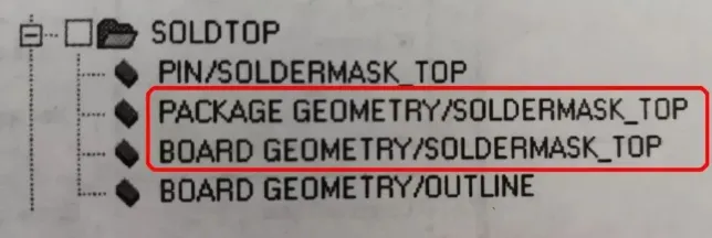
Figure 1 | Example Gerber output dialog showing optional layers.
As a general guideline, typical manufacturing deliverables include at least top and bottom copper, top and bottom solder mask, top and bottom silkscreen (if used), board outline, and drill files (PTH and NPTH). Add internal copper layers for multilayer designs and any special layers required by your process such as carbon ink, peelable mask, or selective gold. Ensure the CAM output matches the fabricator's required file set and naming conventions to avoid misinterpretation.
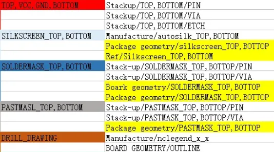
Figure 2 | Gerber setup with selectable sublayers. Optional entries may be omitted if they do not carry required fabrication data.
12. AD14 plugin installation fails; import wizard not found
Use an offline installation method for plugins. Download the plugin installer package first, then configure the installation path in the parameter settings and run the installer. Ensure that the plugin version matches your AD14 build to avoid compatibility issues. If the import wizard is unavailable, verify that the plugin framework is enabled and that the installation paths point to the correct user and program directories.
Additional practical notes
Many of the workflows above benefit from a rules-driven design approach and consistent project templates. Exporting and reusing rule sets, setting up repeatable Gerber outputs, and standardizing test point placement and naming conventions all contribute to predictable SI/PI behavior, smoother DFM, and fewer late-cycle surprises. When versions differ across team members, align on a stable release and shared configuration package to minimize environment-induced discrepancies.
For single-sided designs and via stitching patterns, coordinate early with your PCB fabricator on layer stack, copper weights, mask definitions, and drill limits. Align your rules with those constraints so the tool flags issues during design rather than at CAM review. Finally, keep your system and Altium installation up to date within your organization's validation policy to benefit from stability improvements while maintaining consistent tool behavior across projects.






