Via-in-pad comes up often among new and working PCB designers. The usual question is whether a via can sit directly in a pad, and what happens if it does.
01 | Possible in Theory, Not Preferred in Practice
Two basic points:
First: in theory, a via in the pad gives the shortest lead and the lowest lead inductance, so it is electrically allowed. For some high-speed or high-frequency layouts that looks like the shortest connection.
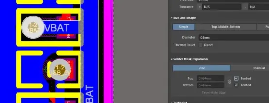
Figure 1 | Structure of a via placed in a pad
Second: from the soldering process, the same structure can cause serious defects.
If the via is not fully plugged, solder paste can run into the hole, the joint can go cold, or the part can lift.
02 | Common Defects: Solder Wicking and Tombstoning
Solder wicking
If the via is not fully closed, solder paste flows down the hole during reflow. The pad is left short of solder, the joint fails, or the mechanical strength is too low.
Tombstoning
When the two ends of a chip part heat unevenly, paste on one side melts first because of wicking or uneven heat. Unbalanced force stands the part up.
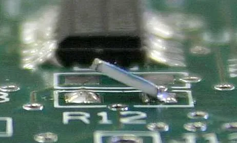
Figure 2 | Tombstoning, with one end of the part lifted
This is especially common on chip resistors and capacitors and is a typical SMT defect.
03 | Two Terms: Lead Inductance and Tombstoning
Lead inductance
In a high-frequency circuit the conductor itself has inductive reactance. The short lead between a via and a pad is a common source of parasitic inductance and can hurt high-speed signaling or power integrity.
In theory, that lead should be as short as possible.
Tombstoning
Also called the Manhattan effect. During soldering of a chip part, unequal force at the two ends lifts one end and the joint fails.
04 | Preferred Practice: Pull the Via Off the Pad
Balancing theory and process, the preferred layout is to pull the via out of the pad and connect it with a short trace.
Benefits:
- Lead inductance stays small
- Process defects are avoided
- Solder yield rises
| Item | Feasibility | Recommendation |
|---|---|---|
| Via in pad | Possible in theory | Not recommended (process risk) |
| Via beside the pad, short trace | Slight extra routing | Recommended (process-friendly) |
Layout is not only drawing a net. It has to carry signal, electrical, and manufacturing constraints together.
Via location is a small choice. It still decides whether the board solders and ships cleanly.