In analog and mixed-signal design, the bipolar junction transistor (BJT) remains a foundational and versatile device. With simple topologies, BJTs can provide level inversion, non-inverting translation through cascaded stages, level shifting across supply domains, and even a degree of inherent “filtering” through their switching behavior. This article walks through several classic circuits, showing how to build inverting and non-inverting logic using NPN and PNP transistors, and clarifies why these stages can suppress small glitches. It also compares NPN, PNP, and complementary NPN+PNP combinations to address typical design questions about compatibility and reliability.
Inverting Level Translation with an NPN Transistor
Figure 1 shows an NPN-based switching stage used as an inverter:
- Input: a 3 V square wave (logic high 3 V, logic low 0 V).
- When the base current Ib ≈ 1 mA, the transistor enters saturation and VCE ≈ 0.3 V (approximated as logic 0 at the output).
- Set R8 = R9 = 2 kΩ; choose R7 based on the load requirements.
The resulting logic is:
- Input high → NPN turns on → collector pulled near ground → output ≈ 0 V.
- Input low → NPN turns off → collector pulled up by the load network → output = +12 V.
Thus, the circuit implements a clean inversion: high-in/low-out and low-in/high-out. Practically, the stage also performs level translation. The input domain operates at 3 V, while the output node is tied to the 12 V rail via the load or pull-up path. When the NPN saturates, its collector is clamped close to ground (VCE(sat) around 0.3 V). When it is off, the collector node rises to +12 V through the load, delivering a full-rail high level to the downstream circuitry.
Design considerations for this stage include selecting base and collector resistors so that the transistor saturates reliably under worst-case conditions without excessive base current. The example uses an Ib of about 1 mA to guarantee saturation when sinking the intended collector current. R7, tied to the output node and +12 V, must be chosen according to the load current and the required rise time. R8 and R9 at 2 kΩ form part of the base drive network; ensure that the base current limit and source drive capability are consistent with the input logic device.
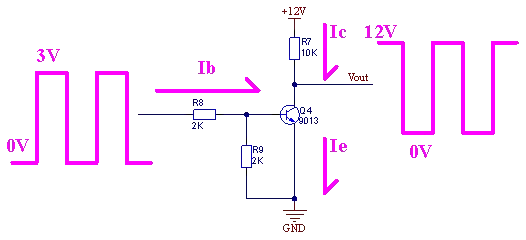
Figure 1 | NPN inverter and level shifter: 3 V logic input drives a 12 V output node through an NPN switch.
Achieving Non-Inverting Behavior with Two Inverting Stages
Non-inverting translation can be achieved by cascading two inverters. Figure 2 illustrates this arrangement using two BJT stages:
- Input high → Q7 turns on → Q6 base is clamped → Q6 turns off → output high.
- Input low → Q7 turns off → Q6 turns on → output low.
By chaining two inversions, the overall polarity is preserved (a “double negative”), while enabling power amplification at the second stage. The first transistor primarily translates logic and provides drive to the second stage. The second stage can be sized to source or sink more current for the load, decoupling the input logic device from heavy output demands.
Two practical points accompany this architecture:
- Propagation delay: Each saturated BJT adds turn-on and, especially, turn-off delay because stored charge must be removed from the base during turn-off. If faster edges are required, avoid deep saturation where possible, and keep base currents just high enough for the intended collector current.
- Bias and pull networks: Provide proper biasing and ensure that intermediate nodes are not left floating. Use resistors sized to set predictable switching thresholds and to avoid unnecessary static current.
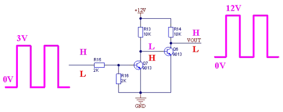
Figure 2 | Cascaded inverters yield non-inverting behavior while allowing the second stage to deliver higher output power.
Why These Switching Stages Exhibit a Filtering Effect
Designers often ask how a simple BJT “switch” can appear to act as a filter. As shown in Figure 3, even if the input square wave contains small spikes or high-frequency interference, the output is not a direct analog copy of the input waveform. Instead, the output node is driven by the 12 V supply through the transistor and load network. This creates two useful effects:
- Logic gating: The BJT conducts only when the base-emitter junction is forward-biased and sufficient base current flows. Small glitches that do not raise the base above the switching threshold long enough fail to switch the transistor, so they do not appear at the output.
- RC time constants and stored charge: The base drive network and the transistor’s intrinsic capacitances (and any bias resistors) form an effective low-pass path from the perspective of fast, narrow pulses. Very brief spikes may be attenuated before they can cause a full logic transition.
This behavior provides a degree of isolation: the output rails are tied to the regulated supply, and the transistor enforces a threshold and timing requirement for transitions. While this is not a substitute for a dedicated filter or a debounce network, it can suppress small, fast disturbances in many logic translation use cases.
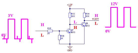
Figure 3 | The output is supply-driven and only switches when the BJT is driven properly, which rejects short input glitches.
Using a PNP Transistor for Inverting Output
A PNP transistor on the high side can also implement inverting behavior, as shown in Figure 4:
- Input low → Q12 turns on → output pulled high (≈ VCC).
- Input high → Q12 turns off → output pulled down by R27 → output low.
This is the high-side complement of the NPN inverter. When the base is sufficiently lower than the emitter, the PNP conducts, sourcing current to the load and producing a high output. When the base is raised closer to the emitter potential, the PNP turns off and the output is pulled low by the load or a pull-down resistor.
In high-side designs, pay attention to input-level compatibility. The PNP base must never be driven beyond its emitter by more than the allowable base-emitter reverse voltage, and the input domain must be able to pull the base high enough to fully turn the PNP off. A proper resistor network ensures controlled base current and safe voltage differentials.
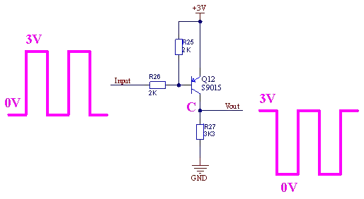
Figure 4 | PNP high-side inverter: input low turns the PNP on to source a high-level output; input high turns it off and the output is pulled low.
Why Two PNP Stages Still Invert in This Topology
Figure 5 connects two PNP stages in series on the high side:
- Input high → Q16 off → Q15 off → output low.
- Input low → Q16 on → Q15 on → output high.
Despite being two stages, this arrangement still behaves as an inverter rather than a non-inverter. The reason lies in the high-side reference of each PNP device. Each stage inverts relative to its own emitter reference. Cascading two such high-side inverters without an intermediate low-side inversion does not produce a net non-inverting response in this configuration. In practice, this structure retains inverting behavior and does not provide the same “double negative equals positive” effect as the earlier NPN–NPN chain tied to ground reference.
Additionally, double high-side stages can complicate base drive referencing and make clean turn-off more difficult if the intermediate node rises near the top rail. For robust non-inverting translation, using complementary devices is often a better choice.
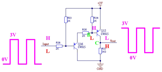
Figure 5 | Two high-side PNP stages arranged as shown still yield an inverting function rather than a non-inverting one.
Solution for Same-Polarity Output: NPN Input Stage + PNP Output Stage
A practical way to achieve non-inverting behavior with a high-side output is to combine an NPN input stage with a PNP output stage, as in Figure 6. The logic sequence is:
- Input high → Q14 (NPN) turns on → node A ≈ 0.3 V → Q13 (PNP) turns on → output high.
- Input low → Q14 turns off → node A rises to approximately +3 V → Q13 turns off → output low.
This arrangement uses the NPN as the input interface to a 3 V logic domain and level-shifts to a PNP that sources the high-side output. It provides a same-polarity transfer function—high-in/high-out and low-in/low-out—while cleanly bridging a 3 V control signal to a higher-voltage load domain. This makes the stage well-suited for microcontroller I/O pins driving loads that require a supply higher than the logic rail.
Design notes for the complementary pair:
- Base bias networks: Provide defined pull-ups/pull-downs so that node A and the PNP base never float. Ensure Q13’s base-emitter differential remains within safe limits under all conditions.
- Current sizing: Choose base resistors to provide sufficient drive for the intended load while avoiding excessive base current. For the NPN, saturating with about 1 mA base current, as in the earlier example, ensures a low node A during “on.”
- Timing and recovery: Complementary stages introduce two switching events; account for added propagation time and, if necessary, limit saturation to reduce storage delay.
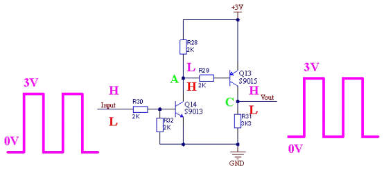
Figure 6 | NPN + PNP complementary pair: non-inverting transfer with a 3 V control input and high-side output drive.
Key Design Takeaways
- NPN-based switch stages naturally implement an inverting transfer. Cascading two inverters restores the original polarity and provides a convenient way to boost output drive.
- Because the output node is driven from the supply through the switching network, these stages can reject small, fast disturbances—acting as a rudimentary “filter” in logic translation scenarios.
- PNP high-side stages can also provide inverting behavior. However, simply stacking two PNP stages on the high side in the shown configuration does not yield a non-inverting output.
- An NPN input stage followed by a PNP output stage is a robust way to achieve same-polarity level translation between a 3 V logic domain and a higher-voltage load domain, improving compatibility and stability.
- Match resistor values and drive strengths to the logic source and the load: ensure base currents are adequate for saturation without overstress, and verify that the chosen thresholds align with the logic family’s VIH/VIL.
A practical rule of thumb: PNP on the high side, NPN on the low side. Applied thoughtfully, this mnemonic helps establish clear design intent, stable biasing, and predictable logic behavior in mixed-voltage BJTs switching circuits.