Power circuits face multiple sources of instability, and purpose-built protection networks are used to prevent those instabilities from damaging equipment or degrading performance. In practical electronics, protection circuits are everywhere, including overcurrent protection, overvoltage protection, overtemperature protection, no-load protection, and short-circuit protection. This article organizes several commonly used protection topologies, explains their operating principles, and highlights their practical considerations.
Motor Overtemperature Protection
Continuous-duty electromechanical equipment such as automatic lathes, industrial ovens, and ball mills, as well as unattended systems, can suffer accidents when a motor overheats or a thermostat fails. A PTC thermistor-based overtemperature protection circuit provides a simple and effective safeguard against such failures.
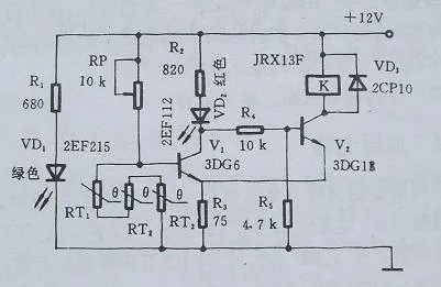
The example below uses a PTC thermistor network and a Schmitt trigger as a control circuit. Three identical step-type PTC thermistors (RT1, RT2, RT3) are embedded in the stator windings. Under normal conditions, these PTCs are at ambient temperature and their total resistance is less than 1 kΩ. In this state, transistor V1 is off, V2 is on, a relay (K) is energized, and its normally open contacts supply mains power to the motor.
When a localized fault causes overheating, the first PTC that exceeds its preset temperature sharply increases its resistance—often above 10 kΩ. V1 then turns on and V2 turns off, a red indicator LED (VD2) lights to signal an alarm, the relay de-energizes, and the motor is disconnected from the mains, achieving thermal protection.
Selecting the PTC depends on the motor's insulation class. A practical guideline is to choose the PTC's Curie temperature approximately 40 °C below the insulation class's maximum temperature. For example, with a Class B motor whose limit is 130 °C, a PTC with a Curie temperature of around 90 °C is appropriate.
Protection in Inverter Power Supplies
Inverters frequently experience significant current transients. If current exceeds the allowed range, key components can be severely stressed or destroyed. Robust protection circuits are therefore critical in inverter designs.
Reverse-Polarity Protection
Without reverse-polarity protection, reversing the battery leads can produce catastrophic damage—from a blown fuse to widespread circuit failure. Common reverse-polarity protection implementations include the following.
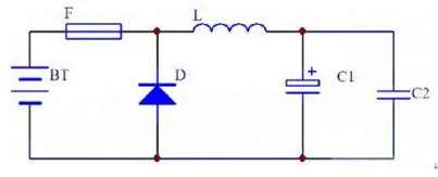
In this approach, a Schottky diode is connected across the input rails so that, if the battery is reversed, the diode conducts and the fuse (F) blows. If a push-pull converter follows, the body diodes of the two MOSFETs are effectively in parallel with the Schottky. Because the Schottky has a lower forward drop and higher surge capability than the MOSFET body diodes, it conducts first, preventing large surge currents through the MOSFETs and thus protecting them. This circuit is simple and does not reduce efficiency during normal operation, but it sacrifices the fuse, which must be replaced after a fault.
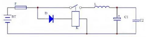
A relay-based reverse-polarity circuit uses a diode and relay coil arrangement such that, with reversed battery polarity, the diode is reverse-biased, no current flows through the coil, and the relay contacts remain open, disconnecting the inverter input. This method avoids blowing the fuse, but it has the drawbacks of larger size and finite contact life.
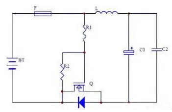
A MOSFET-based reverse-polarity circuit behaves like an ideal diode. In the schematic, D denotes the MOSFET's intrinsic body diode, shown explicitly for analysis. With correct battery polarity, the body diode initially conducts, and the MOSFET's gate-source is forward-biased via F, R1, and D, turning the MOSFET on. Once on, the MOSFET's voltage drop is much lower than the diode's, so the body diode ceases conducting. With reversed polarity, the body diode is reverse-biased, the MOSFET's gate-source is reverse-biased, and the MOSFET remains off, preventing the inverter from powering up. This method uses no mechanical contacts, achieves long life, and avoids blowing a fuse. Its drawback is the MOSFET's conduction loss; selecting a device with suitably low Rds(on) minimizes loss under high current.
Battery Undervoltage Protection
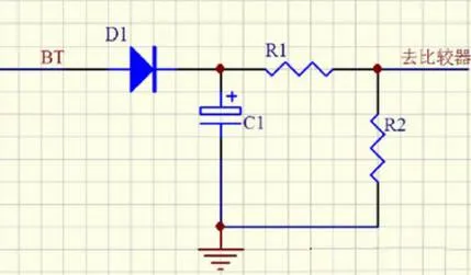
To prevent damaging deep discharge, the inverter should shut down when battery voltage drops below a threshold. If the undervoltage protection is too sensitive, it may trip during startup of high-inrush loads, making it difficult to start such loads—especially when the battery is not fully charged. The circuit below incorporates D1 and C1 to quickly establish the battery sampling voltage and introduce a delay, reducing nuisance trips during transient sag.
Lithium-Ion Battery Charging Protection
Both overcharge and overdischarge degrade lithium-ion battery life. When designing a charger, pay close attention to charge voltage and current limits and select an appropriate charger IC. Implement charge-state indication, temperature-qualified charging, and protection against overcharge, overdischarge, and short circuit. Thorough testing is required to ensure safe operation across conditions.
Charging Circuit Example
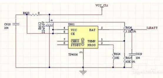
The example below uses a TP4056 linear charger. The maximum charge current is set by a programming resistor. The circuit can implement charge status LEDs and a temperature window so charging only occurs within a defined temperature range.
Protection Circuit Example
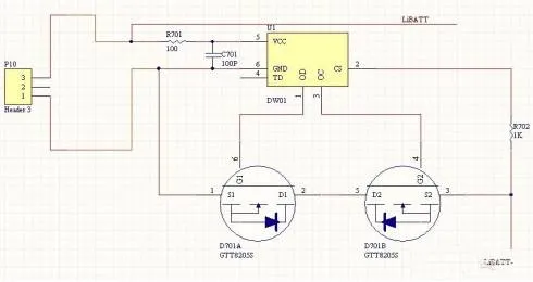
A popular protection front end combines a DW01 protection IC with a dual MOSFET package such as 8205. This combination provides overcharge, overdischarge, and short-circuit protection for single-cell lithium-ion packs.
Overcurrent Protection in Switch-Mode Power Supplies
Common Overcurrent Protection (OCP) Characteristics
Overcurrent protection can be implemented with several characteristic behaviors, as shown in Figure 1. These include:
- Fold-back current limiting (current droops as output voltage falls).
- Constant-current limiting.
- Constant-power limiting.
Most power supplies adopt a fold-back characteristic. The OCP setpoint is typically 110% to 130% of the rated current, and most designs recover automatically when the fault is cleared.
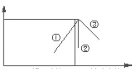
Figure 1 | Overcurrent protection characteristics: 1 — fold-back, 2 — constant-current, 3 — constant-power
Current Limiting for Directly Driven Transformer Primaries
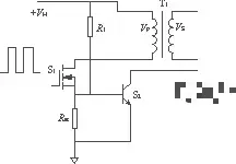
In single-ended forward and flyback converters where the transformer primary is directly driven, current limiting is relatively straightforward. Figure 2 illustrates two methods. In both Figure 2(a) and 2(b), a sense resistor Rsc is inserted in the MOSFET source.
In Figure 2(a), the voltage across Rsc drives transistor S2. In Figure 2(b), a comparator senses the voltage across Rsc and, when an overcurrent threshold is reached, truncates the drive pulse to protect the switch. Compared with the transistor-only scheme, the comparator-based solution is faster and more accurate: it sets a precise threshold (typically 100 mV to 200 mV), allowing Rsc to be smaller, thereby reducing power loss and improving efficiency.
When the AC input spans 90 to 264 V with the same output power, primary peak currents differ significantly, causing the OCP point to drift between high- and low-line conditions. Adding a pull-up resistor R1 from +VH establishes a preset bias at the base of S2 or at the comparator's non-inverting input, aligning the OCP trip point across the input range as closely as practical.
(a) Transistor protection
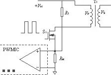
(b) Comparator protection
Figure 2 | Current-limiting circuits in single-ended forward and flyback converters
Base-Drive Current Limiting
In many designs, the base-drive circuit isolates the control circuitry from the power switch, while the control and output stages share a ground reference. The current limit can be tied directly to the output side, as shown in Figure 3, and operates as follows.
During normal operation, the voltage across Rsc generated by the load current IL is below the threshold required to turn on S1. With S1 off, IC1 charges are zero, capacitor C1 is uncharged, and S2 remains off. As IL rises to the setpoint such that ILRsc = Vbe1 + Ib1R1, S1 turns on and charges C1 with a time constant τ = R2C1. After charging, the voltage on C1 reaches VC1 = Ib2R4 + Vbe2. To ensure rapid discharge of C1 when an overcurrent is detected and to enable quick reset after the fault clears, choose R4 to provide an appropriate discharge path.
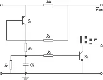
Figure 3 | Current-limiting circuit applicable to multiple converter topologies
Lossless Current Limiting Using a Current Transformer
While the preceding techniques are effective, the sense resistor Rsc dissipates power and reduces efficiency, especially at high output currents. The circuit in Figure 4 uses a current transformer (CT) as the sensing element, enabling efficient current detection with negligible series loss.
The CT T2 senses load current IL in its primary and couples a proportional current into the secondary, producing a voltage across R1. Diode D3 rectifies the pulses, and R2 and C1 provide smoothing. Under overload, the voltage across C1 rises quickly, a Zener diode D4 conducts, and transistor S1 turns on. The signal at S1's collector can be fed to the converter's control loop as a shutdown or duty-cycle reduction signal.
CTs can be wound on ferrite or MPP toroidal cores and must be tested to avoid core saturation. Ideally, the turns ratio corresponds to the desired current ratio. A practical first estimate for winding is Np = 1 and Ns = NpIpR1/(Vs + VD3). Final turns and component values should be verified and adjusted experimentally to achieve the best performance.
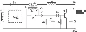
Figure 4 | Lossless current-limiting circuit
Using a 555 Timer for Current Limiting and Hiccup Operation
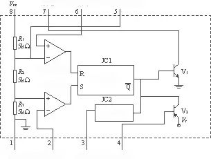
Figure 5 shows the functional block diagram of the 555 timer. The 555 is a versatile analog IC family (e.g., LM555, RCA555, 5G1555) used in delay circuits, monostable and astable oscillators, pulse modulation, and can serve in converter control circuits.
Internally, the 555 includes a three-resistor divider (R1, R2, R3), two comparators, an R-S latch, and two transistors. It operates from 5 to 18 V. The divider provides 2Vcc/3 to comparator 1's inverting input and Vcc/3 to comparator 2's non-inverting input. Pins 2 and 6 are the trigger and threshold inputs, respectively. The comparators drive the latch, whose output controls the discharge transistor (pin 7) and the output stage. When the latch output is high, the discharge transistor turns on, pulling pin 7 low; when low, the discharge transistor turns off and the output stage presents a low impedance. The 555 output stage can source or sink up to approximately 200 mA. A PNP transistor referenced to an internal Vr provides a reset function; when pin 4 (reset) is tied to Vcc, this PNP is reverse-biased and off.
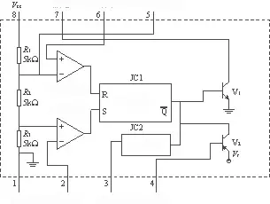
Figure 5 | Basic block diagram of a 555 timer
Figure 6 shows a current-limit protection circuit using a 555 to implement hiccup-mode protection. UC384X, S1, and T1 form a basic PWM converter. The UC384X-series controller employs two control loops: an output-voltage feedback loop (error amplifier compared to a reference Vref; in this example pin 2 is grounded directly to prevent self-oscillation in the error amplifier), and a current loop that senses the transformer primary current via T2's secondary, filtering on R8 and C7, and compares the resulting voltage to the error signal to modulate pulse width at a fixed clock frequency.
UC384X offers excellent line regulation (~0.01%/V), improved load regulation, simplified compensation of the error amplifier with better stability and frequency response, and a high gain-bandwidth product. It supports two shutdown mechanisms: raising pin 3 above 1 V to trip overcurrent and shut off the output, or pulling pin 1 below 1 V so that the PWM comparator output forces the latch to reset and disable output until the next clock pulse sets it again.
The CT T2 monitors the primary peak current in T1. During overload, the peak current rises rapidly; T2's secondary current increases, D1 rectifies, and R9/C7 smooth the signal delivered to IC1's pin 3. This drives IC1's control to reduce or shut down output. Note: components R3 and C4 connected to IC1 pin 1 must be configured in open-loop mode; if closed-loop, the 555's pin 7 discharge path cannot function correctly during overcurrent.
IC1's pin 1 is tied to IC2's (555) pin 6; as the 555's comparator input falls, the latch output Q goes high, turning on the discharge transistor at pin 7, pulling IC1's pin 1 below 1 V. IC1 output then shuts down, S1 receives no gate drive, and the converter stops. If the overcurrent persists, the sequence repeats and the converter operates in a repeating start–stop cycle—hiccup mode. During overload, the off-time is long and the on-time is short, limiting thermal stress. The hiccup period is determined by the 555 monostable's RC time constant τ = R1C1. When the overload clears, normal operation resumes. T2 selection and calculation follow the same method described for the lossless CT current limiter.
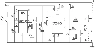
Figure 6 | Current-limit protection using a 555 to enforce hiccup operation
Comparison of Overcurrent Protection Methods
The table below summarizes and compares the characteristics of several current-limiting methods discussed above.
These circuit families cover a wide range of use cases across motors, inverters, lithium-ion charging systems, and switch-mode power supplies. Selecting among them involves balancing protection robustness, efficiency, cost, complexity, and recovery behavior under real-world faults and transients.