










In high-speed PCB design, DDR is a critical subsystem that cannot be treated casually. Whether you are using DDR, DDR2, or DDR3, insufficient rigor in PCB design often leads to impedance discontinuities, reflections, distorted waveforms, timing violations, and unstable systems.
This article focuses on practical DDR PCB design essentials. It covers definitions, impedance targets, layout topologies, routing control, and skew budgeting, supported by illustrative diagrams.
What Is DDR?
DDR (Double Data Rate) is a type of synchronous DRAM that transfers data on both the rising and falling edges of the clock. For a given clock frequency, this doubles the data transfer rate compared to single data rate interfaces.
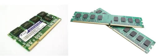
Figure 1 | Conceptual illustration of DDR memory
Common generations include DDR, DDR2, DDR3, and DDR4.
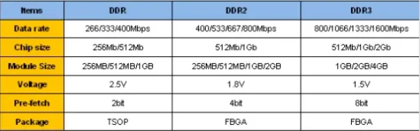
Figure 2 | Representative DDR memory generations
Because both the rising and falling edges of the clock can be used to transmit data, the effective throughput doubles for the same clock frequency.
Impedance Control Requirements
DDR PCB traces must be routed with controlled impedance. Typical targets are:
- Single-ended signals: 50 Ω
- Differential pairs: 100 Ω
Impedance mismatch causes reflections and waveform distortion, which in turn lead to timing anomalies and margin loss. Impedance control is not optional.
DDR Layout Topologies and Design Guidelines
DDR layout topologies depend on how many memory devices are attached to the controller. Selecting an appropriate topology is a key decision that directly affects signal integrity, skew, and timing closure.
A. Single Memory Device (Point-to-Point)
Use a point-to-point connection between the controller and one DDR device, with the following practices:
- Place the memory close to the controller.
- Arrange data banks as symmetrically as practical.
- Use a recommended spacing in the range of 500–800 mil.
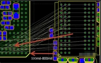
Figure 3 | Example of point-to-point layout for a single DDR device
B. Two Memory Devices (T-Topology)
For two devices, a symmetric T-topology is recommended to equalize path lengths:
- Distribute the two devices symmetrically relative to the controller.
- Keep the trunk segment L1 identical for both branches; make branch segments L2 and L3 equal in length.
- Meet the length-balance condition: L1 + L2 = L1 + L3.
The split of the routes is illustrated below.
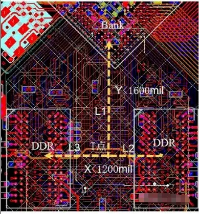
Figure 4 | T-topology for two DDR devices
C. Four Memory Devices
Common topologies for four devices include the following:
Symmetric T-Topology
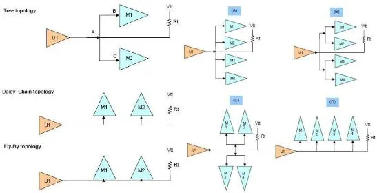
Figure 5 | Symmetric T topology for four DDR devices
Branched T-Topology
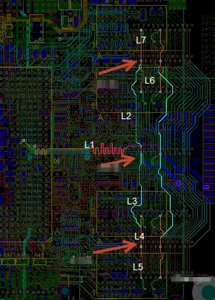
Figure 6 | Branched T topology
Daisy Chain (Fly-by) Topology
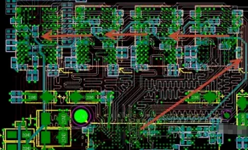
Figure 7 | Fly-by topology (daisy chain)
For DDR3 and higher data rates (e.g., 1600 Mbps), a fly-by topology is generally preferred because it reduces simultaneous stub loading and improves signal integrity.
D. Hybrid Topologies
When PCB space is constrained, a hybrid approach that combines T-topology with fly-by segments can be used. In such cases, enforce strict length matching on the branches to preserve timing alignment. For example, balance the path lengths according to:
L1 + L3 + L2 = L1 + L4 + L5
A typical hybrid topology example is shown below.
Figure 8 | Hybrid topology combining T and fly-by
Signal Grouping and Routing Rules
The following guidelines use a four-device DDR3 configuration as an example, focusing on practical routing control and skew budgeting.
A. Data Bus Grouping
The data interface consists of 32 data lines (DATA0–DATA31), four data masks (DQM0–DQM3), and four differential data strobe pairs (DQS0P/DQS0M through DQS3P/DQS3M). These 36 single-ended lines and 4 differential pairs are partitioned into four data groups for routing and skew control.
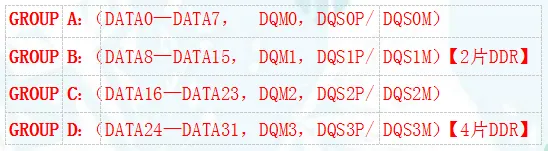
Figure 9 | Grouping of data, DQM, and DQS pairs
B. Clock, Address/Command, and Control Timing Relationship
The controller launches Address/Command and Control signals relative to the clock, and the DDR devices latch these on the appropriate clock edge. Because Address/Command and Control buses are time-referenced to CLK, the relative propagation delay between CLK and these buses must be tightly controlled. Length-match these nets to achieve the required setup/hold time at the memory devices. Maintaining this relationship is essential to preserving timing margins at the receiver.
C. Skew and Matching Targets
- Differential pair intra-pair skew: keep within 5 mil wherever possible.
- Data group intra-group skew: target within ±25 mil.
- Inter-group skew between data groups: target within ±50 mil.
- Address/Command and Control relative to CLK: length-match to CLK within ±100 mil.
These budgets help maintain timing alignment among related signals and improve both eye opening and sampling margin at the memory interface.
D. Spacing Guidelines
Apply the 3W spacing rule for data lines to mitigate crosstalk. For control and address buses, spacing may be relaxed slightly to 2W–3W when necessary. Keep other traces at least 20 mil or 3W away from clock lines, whichever is greater, to minimize coupling into the clock.
E. VREF Network Design
- Place VREF decoupling capacitors close to the relevant pins.
- Route VREF as short as possible and isolate it from data lines on the same and adjacent layers to reduce crosstalk.
- Use a trace width of at least 15 mil for VREF.
Reference Plane Planning in the DDR Region
Provide a continuous and uninterrupted reference plane under the DDR routing region. Avoid splits, voids, or slots under critical nets, particularly for CLK, DQS, and the Address/Command buses, to maintain uniform return current paths and consistent impedance.
Figure 11 | Ensure a continuous, dedicated reference plane in the DDR region

Figure 12 | Example of contiguous reference layers beneath DDR nets






