










Purpose of termination resistors
In DDR designs, daisy-chain (fly-by) topologies are widely used for layout flexibility, but longer transmission lines introduce reflections that degrade signals. Termination resistors are used to reduce these reflections by matching impedances between the driver, trace, and load.
Common termination approaches include:
- Source series resistors: address reflections at the driver end.
- Parallel termination at the far end: "absorb" reflections at the signal end (this report focuses on this approach).
Measured case: dual-channel DDR3 comparison
The test subject is a dual-channel DDR3 fly-by topology with one driver and eight DRAM devices on each channel. We selected address line A3 for simulation in SigXplorer. The excitation frequency was 533 MHz, and eye diagrams were used to evaluate signal quality. Larger eye width and height indicate more stable signals.
The termination arrangement is shown below.
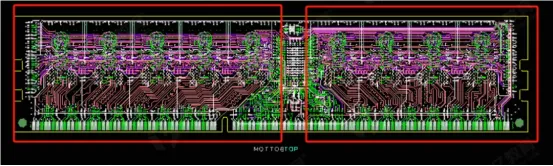
Figure 1 (signal-end termination resistor schematic)
The overall topology: the signal leaves driver U21 and passes through eight DDR devices (U14, U5, U6, U15, U7, U16, U8, U17), with a 39 Ω termination resistor RN106 at the far end.
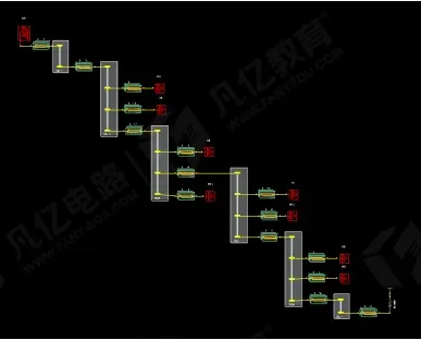
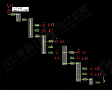
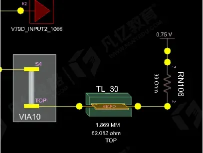
Figure 2 (DDR3 fly-by topology schematic)
Case 1: With termination resistor
The eye diagrams with the termination resistor in place show clear eye width and height (Figures 3 and 4). Overall the signal is effective and does not cross the input thresholds VIH or VIL.
There are small differences depending on device position:
- Devices near the driver (U5, U14): better signal quality, minimal overshoot/undershoot.
- Devices near the far-end termination: more apparent overshoot and undershoot, slightly worse signal quality but still within acceptable limits.
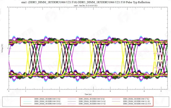
Figure 3 (Eye diagram of address line A3 with termination)
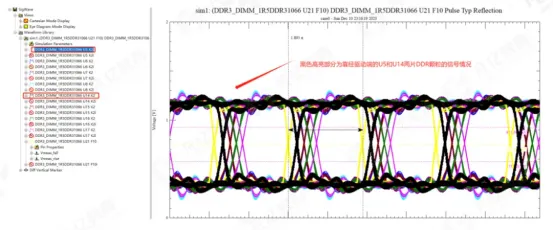
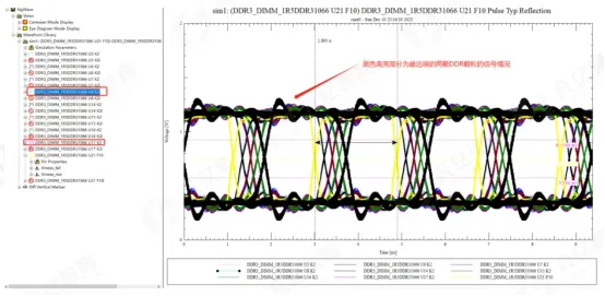
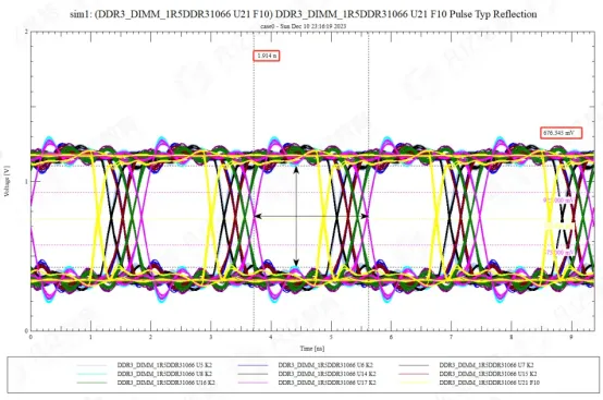
Figure 4 (Signal comparison at different device positions with termination)
Case 2: Without termination resistor
The eye diagrams without the termination resistor show a clear degradation (Figure 5):
- Overall eye width and eye height are much narrower; the valid time between VIH and VIL is short, indicating poor signal quality.
- Counterintuitively, devices near the driver appear heavily distorted with noisy eye diagrams, while the far-end devices show relatively clearer eyes (but still with significant overshoot and undershoot).
This behavior results from reflections traveling back and forth along the trace. Near-end signals suffer from severe interference due to multiple reflected wavelets, while the far end temporarily experiences fewer superpositions, giving a superficially better but still unacceptable waveform.
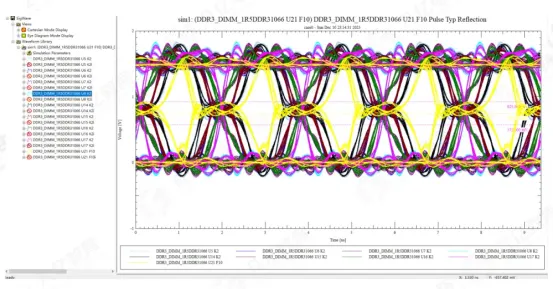
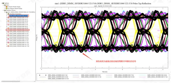
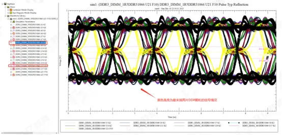
Figure 5 (Eye diagrams and position comparison without termination)
Conclusion
Simulation results indicate that when using a fly-by topology, far-end termination resistors should be applied; otherwise, signal integrity degrades significantly and may prevent correct DDR operation. It is important to select a termination resistance that matches the transmission line impedance to achieve optimal reflection damping.






