










Hardware teams often lose calendar time when a finished product fails EMI and the board keeps changing. Filtering and grounding are the two most practical, most direct tools. Once those two are understood, corrective work becomes much faster.
1. Find Where the EMI Comes From
Before adding parts, identify the source. Extra filters and extra ground traces are guesswork if the path is unknown. Electromagnetic interference splits into conducted interference and radiated interference. Conducted interference travels on power and signal lines. Radiated interference leaves through space. The fixes differ: conduction is a filtering problem; radiation is a shielding and grounding problem.
In project work, about 90% of EMI problems start as conducted energy. The power port and the signal ports are the usual entries. Fix those two first and most of the campaign is done. Much of the remaining 10% of radiation is secondary radiation from a conducted problem, so conducted work stays first.
2. Filtering: The Most Direct, Lowest-Cost Step
2.1 Power-port filtering
The power entry is the largest door into the system. Filtering there has to work. Common-mode filters and differential-mode filters are the two basic blocks. A common-mode filter targets common-mode noise. A differential-mode filter targets differential-mode noise. A π filter added first often does little because common-mode and differential-mode were never separated.
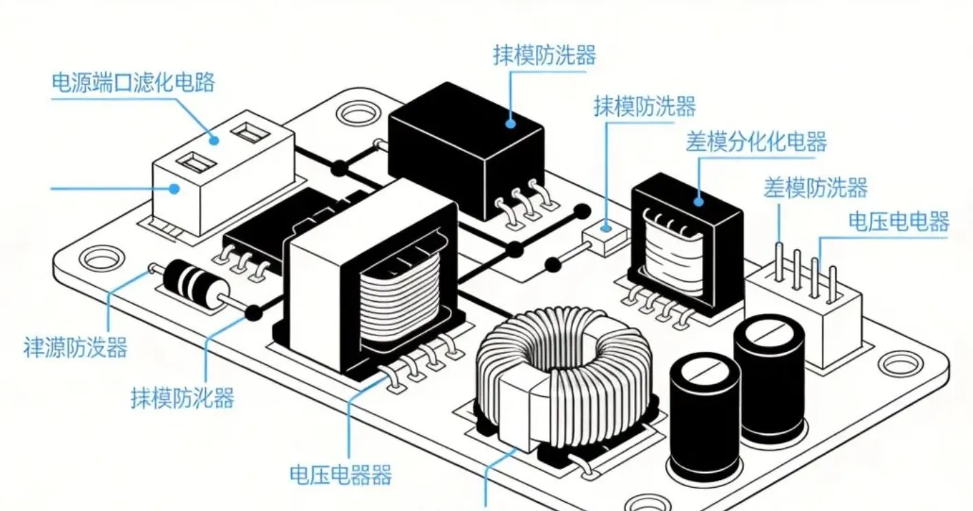
The check is straightforward. Measure with a differential probe and a single-ended probe and read the spectrum. Common-mode noise has the same amplitude and phase on both lines. Differential-mode noise has the same amplitude and opposite phase. Choose the filter after the type is known. Check rated current, voltage rating, and insertion loss. Do not select on price alone.
2.2 Signal-port filtering
Signal-line filtering is more particular than power-line filtering. The wrong capacitor can raise the interference. A ferrite bead plus a capacitor is the usual pair. The bead blocks high-frequency current. The capacitor shunts the high-frequency component to ground. Bead type and location decide the result. A bead in the middle of a signal line can ruin signal quality and still leave EMI almost unchanged.
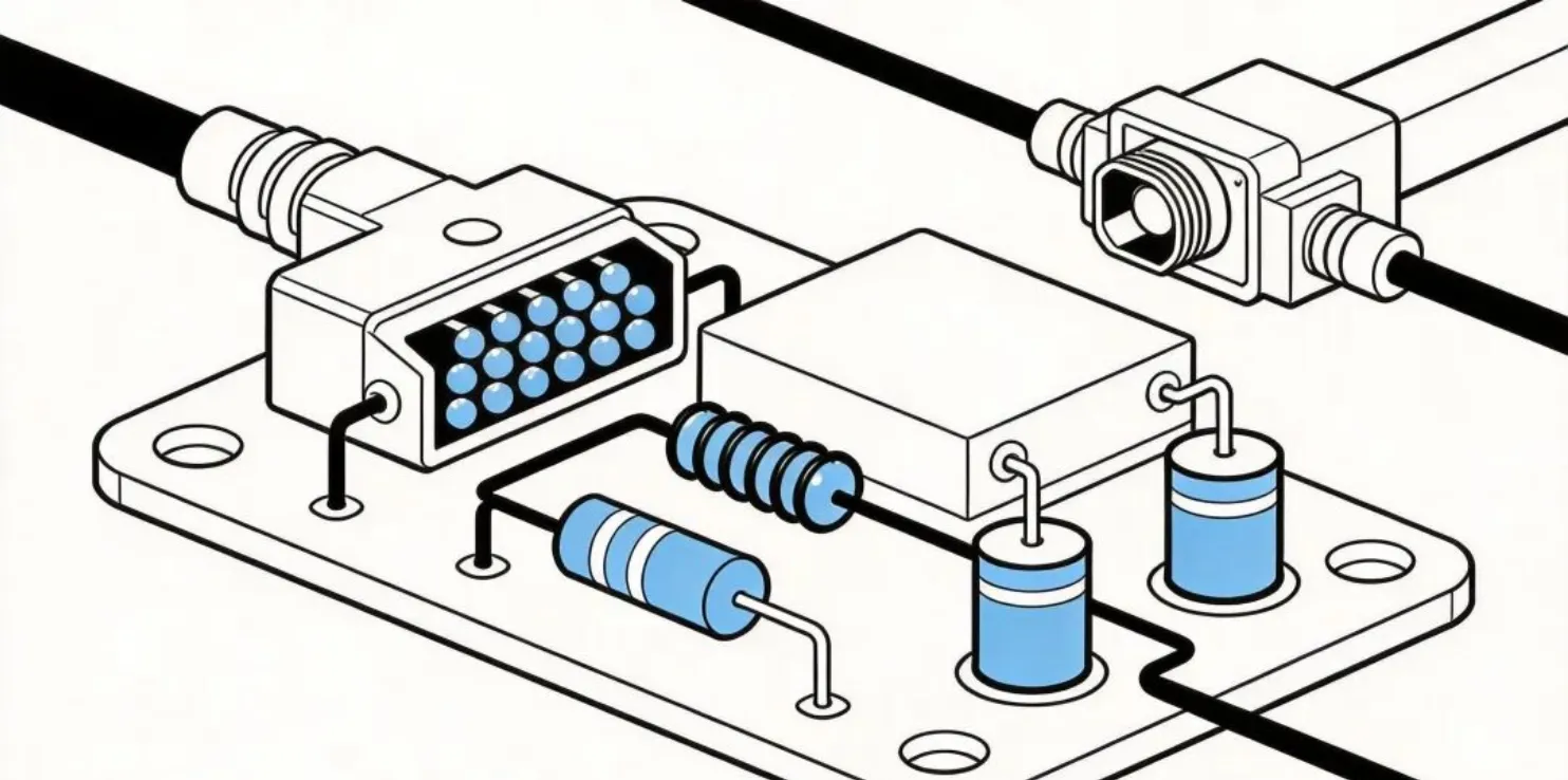
Place the bead next to the connector. Closer is better. Place the capacitor between the bead and the IC. Do not reverse that order. On a low-speed signal, an RC filter often works better than a capacitor alone, because the resistor adds damping and limits resonance.
2.3 Filter-part placement
Layout owns about half of the filter result. The bill of materials can be correct and the filter still do nothing if the placement is wrong. Filter-capacitor traces must be short, wide, and straight. The ground path should drop into the ground plane. Do not route it around the board.
A working rule: put the filter capacitor as close to the IC pin as possible, use as much width as the area allows, and add ground vias generously. Above 30 MHz, trace inductance becomes obvious. A 1 mm run and a 0.5 mm run can differ by several dB. Anyone who has done corrective work has seen that gap.
3. Grounding: Simple on Paper, Detailed on the Board
3.1 Single-point versus multipoint grounding
Textbooks describe single-point and multipoint grounding, and the choice still confuses practice. A working split is: single-point grounding below 1 MHz, multipoint grounding above 10 MHz, and a case-by-case choice between 1 MHz and 10 MHz. The boundary is not rigid, but the direction is.
Single-point grounding avoids a ground loop. Long leads add inductance and become a problem at high frequency. Multipoint grounding works better at high frequency and can form loops. A common compromise is to gather the low-frequency returns at one point and pour a large ground area for the high-frequency returns.
3.2 Analog ground and digital ground
Whether analog ground and digital ground should be split depends on the circuit. If the analog section is noise-sensitive-an ADC front end or a precision amplifier-a split reduces coupling from digital switching. If the board is all digital, the split only adds layout complexity.
When the planes are split, the single-point join matters. Join them near the analog-digital boundary device, such as an ADC or DAC, not at the power entry. A ferrite bead at the power entry is a common substitute. At high frequency that bead still couples, and the isolation is weaker than it looks.
3.3 Ground loops
A ground loop is a common source of both conducted and radiated EMI. Two ground points form a loop. An external magnetic field induces current in that loop, and the current radiates. The usual fixes are to break the loop, raise its impedance, or choose a better ground point.
In practice, choosing the ground point is the more usable path. Floating a ground is one option, with safety and parasitic capacitance kept in view. The most practical step is to put the ground point where the distance between the noise source and the sensitive circuit is shortest, so loop area stays small.
4. Corrective Sequence and Common Traps
4.1 Where to start
A failing plot often leads to random capacitors and beads. A better order is: power first, then signals; near first, then far; low frequency first, then high frequency. Finish conducted emissions at the power port before reading radiated emissions. Treat sources near the board edge before sources farther inboard.
Before changing parts, use a spectrum analyzer to locate the source: power port or signal port, LO leakage or clock harmonic. Changing parts without that location wastes time. A near-field probe with a spectrum analyzer finds radiation hot spots quickly.
4.2 Common mistakes
First mistake: more filters are better. If the filter impedance does not match the system, some bands get worse. A filter is chosen to suppress a known path. It is not stacked by count.
Second mistake: a thicker ground trace is always better. A thick trace has low DC resistance and still has high-frequency inductance. Above 1 GHz a thick trace and a thin trace are not far apart. At high frequency a continuous ground plane is worth more than a thick trace.
Third mistake: shielding solves everything. Shielding can work, but it contains the energy. It does not remove it. An internal source can still couple onto a cable. Opening the can can leave the same problem. Use shielding with filtering, not in place of it.
4.3 Lower-cost options
When chamber time and budget are limited, a ferrite bead plus a capacitor is often the best cost-to-result pair. Cost is low, debug is easy, and most conducted problems respond to it. A low-cost bead and a small capacitor clear a large share of conducted failures.
For radiation, spread-spectrum clocking is useful. Adding spread spectrum on the clock device can drop a radiation peak by more than 10 dB at almost no extra cost. A small shift in switch-mode frequency can also move a peak.
5. Do Not Skip Verification
After the change, measure it. Record how many dB the filter actually removed. Corrective work without numbers cannot be traced. Keep before-and-after data for later analysis.
Without a full instrument set, an oscilloscope plus a near-field probe still gives a direction check: whether the waveform improved and whether a hot spot dropped. That is not a chamber result, but it shows whether the path is right.
Summary
EMI corrective work is hard when the source is unknown and simpler when filtering and grounding are applied in order. Separate conducted from radiated energy, start at the power and signal ports, and half the work is already pointed the right way.
The rest is repetition: change, measure, record. The sequence that holds is: understand the path, choose the part, place it correctly, and verify the result.






