










In PCB design, have you ever spent time hunting for a single component, or struggled to arrange a dense cluster of parts into a more reasonable placement?
Two techniques can improve layout efficiency substantially: interactive placement and modular placement. Used together, they speed up component placement and keep the design logically organized.
Interactive Placement: Linking the Schematic and the PCB
"Select what you see, and the other view follows." That is the essence of interactive placement.
After Cross Select Mode is enabled in both the schematic and the PCB, clicking a component in the schematic highlights the same part in the PCB view, and the reverse is also true. There is no need to search back and forth. One action locates the part on both sides.
How to Enable Cross Select Mode
Two steps are enough:
-
In the schematic view, click the menu: Tools → Cross Select Mode
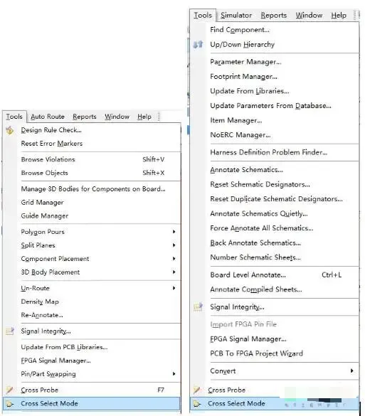
Figure 1 | Cross Select Mode
Repeat the same operation in the PCB view
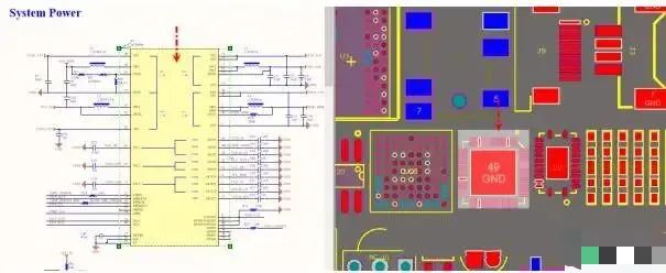
Figure 2 | Selection in cross-select mode
After it is enabled, selecting any component produces an immediate response in the other view and reduces search time.
Modular Placement: Arranging Scattered Parts by Functional Block
If the goal is to gather the parts of one functional module in one area so the layout is easier to read, modular placement is the direct approach.
A useful command for this is Arrange Components Inside Area. It places a selected group of components neatly inside a specified region and is especially helpful in the early stage, when the board is first divided into modules with arrange within a room.
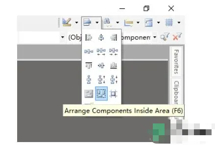
Figure 3 | Arrange Components Inside Area
Procedure
- Select the module: In the schematic, use interactive placement to box-select one functional module.
- PCB follows: In the PCB view, all components belonging to that module are selected automatically.
- Arrange the group: Use Arrange Components to place those parts quickly and neatly.
- Refine the placement: Further optimize the arrangement of ICs, resistors, capacitors, and other parts.
The result is shown below. Each functional module is in order, and the PCB layout is both clearer and faster to complete.
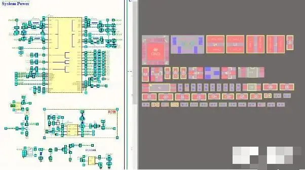
Figure 4 | Modular placement result
Tip: Use Split Vertical to display the schematic and PCB side by side so you can select in one view and place in the other. Design complexity is manageable; disorder is not. The right tools keep the layout orderly.






