










A stable supply is required if an electronic product is to run as designed. The LDO (low-dropout regulator) is a common power-management part, and its PCB layout affects the rest of the circuit. The same rules apply on mobile devices, communications hardware, and embedded boards: placement and routing of the LDO set how stable and quiet the rail is. The sections below start from the LDO's behavior, then cover a typical application circuit and the layout and routing points that follow from it.
What an LDO Module Is, and What It Offers
Before the PCB is drawn, the role of the LDO should be clear. An LDO (low-dropout regulator) is an electronic block made of a DC voltage regulator and a current amplifier. Its job is to take a higher input voltage down to a lower, regulated voltage for the downstream circuit.
Compared with other regulators, four traits explain why LDOs are used so widely:
- Low dropout. Dropout is typically a few hundred millivolts to a few volts, so a higher rail can be brought down to the target low voltage for many low-voltage ICs.
- Output stability. The output is held against input-voltage movement and has useful noise and interference rejection, which reduces faults caused by a moving rail.
- Low power. The regulator is linear and does not switch. Dissipation is lower than that of a switching regulator, which suits power-sensitive mobile products.
- Fast load response. On a sudden load step the LDO can correct the output quickly, limiting sag or overshoot so the load rail stays usable.
Typical Application Circuit: AMS1117-3.3
The widely used AMS1117-3.3 is a clear example of the input–regulate–output path and is the framework for the PCB work that follows.
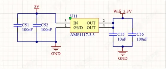
In the schematic, AMS1117-3.3 is the core device. The input (IN) is 5 V. The output (OUT) is a regulated 3.3 V net labeled Wif_3.3V, intended for a 3.3 V load such as a Wi-Fi module. Several capacitors provide filtering:
- Input: two 100 nF capacitors in parallel (C51, C52) remove high-frequency noise on the incoming rail so that noise does not enter the regulator.
- Output: one 100 nF capacitor (C55) in parallel with one 10 μF capacitor (C56). The 10 μF part takes out low-frequency ripple; the 100 nF part suppresses high-frequency noise so the outgoing rail stays smooth.
- Ground: the device GND pin must tie solidly to circuit ground so the current loop is complete and a shifted ground potential does not upset the circuit.
Two Placement Rules for an LDO Power Rail
Placement is the skeleton of the LDO design. A poor arrangement lengthens the power loop and raises noise, which shows up in regulation. Two rules from practice should be followed.
1. Prefer an In-Line or L-Shaped Placement to Keep the Power Loop Small
The LDO power loop (input → device → output) sets both noise and loss. A smaller loop area means less interference and higher efficiency. Placement should therefore satisfy:
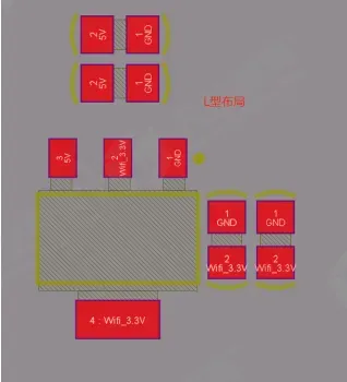
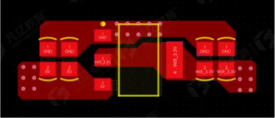
- In-line placement. Arrange input filter capacitor → LDO → output filter capacitor in a straight line so the power path is short and does not detour. This fits boards with enough space and a single routing direction. Loop resistance and parasitic inductance stay down, and IR drop is reduced.
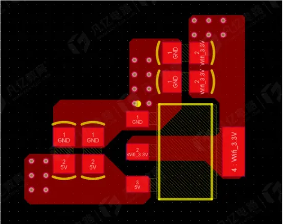
- L-shaped placement. When space is tight, as in a small product, the input and output directions can bend 90°, but the input → device → output path must stay continuous and must not loop around. One example is the input capacitor on the left, the device in the center, and the output capacitor below, forming an L. That saves area and still limits loop size.
2. Place Capacitors Large Then Small
Capacitor order affects filtering. Place parts by descending capacitance, close to the matching device pin:
- Input: if a bulk capacitor is used (10 μF or larger), put it first against the input pin to remove low-frequency ripple. Place a small capacitor (for example 100 nF) next to that bulk part to cut high-frequency noise so the voltage entering the device is clean.
- Output: the same order applies. Put the bulk capacitor (for example 10 μF) next to the output pin to remove low-frequency ripple after regulation, then parallel a small capacitor (for example 100 nF) to remove high-frequency noise so the 3.3 V delivered to the load (such as a Wi-Fi module) does not move.
Four Routing Rules for an LDO Power Rail
If placement is the skeleton, routing is the current path. Bad routing causes IR drop, sag, and noise coupling. The four points below are the ones that prevent most of those failures.
1. Size the Power Path for the Current
Trace width and via count on the input and output must be calculated from the LDO's actual maximum operating current. A common estimate is 1 A per 1 mm of width on 1 oz copper; with heavier copper the width can be reduced. If the LDO can deliver 2 A, input and output traces should be no narrower than 2 mm, with at least two vias (about 1 A per via). Too little width or too few vias heats the path, drops voltage, and can open the copper.
2. Put Vias Before the First Input Cap and After the Last Output Cap
Via location affects filtering. A via in the wrong place lets unfiltered voltage into the device, or puts noise back onto a rail that was already regulated:
- Input via: place it before the first input filter capacitor. The external 5 V should pass through the via, then into the input capacitors, then into the LDO, so via parasitics are filtered before the device.
- Output via: place it after the last output filter capacitor. The 3.3 V from the device should go through all output capacitors first, then through the via to the load (such as a Wi-Fi module), so the load sees a filtered rail.
3. GND Routing: Wide Return and Vias Next to the GND Pin
Ground is the return path. A poor ground produces ground bounce (a short shift in ground potential) and moves the output. GND routing should follow:
- Return width: GND traces should match the power-trace width and should not be narrower. If the power trace is 2 mm, GND should be ≥ 2 mm so return current is not forced through a high-resistance path that splits ground potential.
- Via location: put GND vias next to the LDO GND pin. The closer the via is to that pin, the smaller the ground loop, which reduces ground bounce and keeps noise from coupling through ground into the 3.3 V rail.
4. Tie Input Ground and Output Ground Together
Ground on the input side (input-capacitor ground and the input loop) and ground on the output side (output-capacitor ground and the load ground) must connect directly and share one ground reference. If input ground and output ground are split, a potential difference appears between them and the output can drift (for example 3.3 V becoming 3.1 V or 3.5 V), which upsets the load. In the layout, join input ground and output ground with a wide copper pour, or tie both into the same ground plane so the two nodes sit at the same potential.
Summary
LDO power PCB design reduces to a short loop, effective filtering, and a solid ground. An in-line or L-shaped placement shortens the power path. Large-then-small capacitors cover low- and high-frequency noise. Routing that is sized for current, with vias in the right place, a wide nearby ground, and input and output grounds tied together, keeps current moving and ground potential still.
Used with the figures above, those placement and routing rules address rail movement, coupled noise, and excess dissipation. Special cases such as a high-power load or a very small board may need different values, but the same three constraints still apply: shrink the loop, finish the filtering, and keep ground stable.






