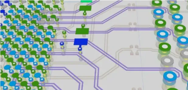
LDO linear regulators often show large output ripple and high package temperature. The layout points below address those two symptoms together.
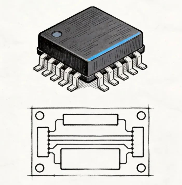
Noise Control Comes First
LDO noise mainly comes from parasitics at the input and output and from ground-loop interference.
The first step is input-capacitor placement: a 10 μF electrolytic capacitor plus a 0.1 μF ceramic capacitor, tight against the LDO input pin, to reduce input impedance.
The second step is output-capacitor placement: put the output capacitor as close to the output pin as possible so parasitic inductance does not slow the regulator's response.
The third step is the ground plane: a continuous ground plane is the baseline. Join input and output grounds at one point and avoid a ground loop.
The fourth step is signal clearance: keep sensitive nets away from the LDO power region, widen the power traces, and shield critical signals.
Thermal Design Cannot Be Skipped
Copper for heat spreading is the first thermal step. Pour a large copper area under the LDO. Copper weight should be ≥1 oz, and the pour should connect to multiple ground-plane layers when possible.
Thermal vias matter as well. In the heat-spreading region use a 4×4 or 5×5 via array, 0.3-0.5 mm drill, spaced evenly.
Match thermal resistance with care. Choose a low-θJA package, use the datasheet thermal-resistance values, and leave 20% thermal margin.
Choose the package for the power level. Use TO-220 for higher power and SOT-223 for medium power. Do not run the part overloaded.
Measurement is the check that counts. Use infrared temperature measurement to find hot spots. At 25 °C ambient, die or case temperature should stay below 85 °C. Measure output ripple with an oscilloscope and confirm the system is stable.
Summary
Four points hold the design together: capacitor placement, a continuous ground plane, thermal copper and vias, and measurement after the board is built.
Use these placement rules, simulate ahead in the EDA tool where possible, and verify on the prototype. Then fold the results into a local PCB design checklist.