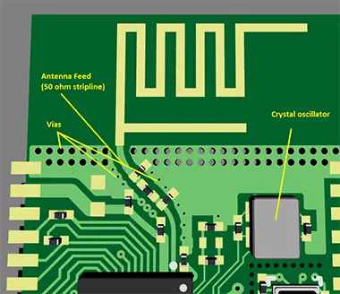
Decoding PCB Schematics: A Guide for Effective Diagnostics
Master decoding PCB schematics with this practical hobbyist guide. Learn standard symbols, circuit tracing techniques, fault finding with schematics, key differences between PCB layout vs schematic, and best practices for effective diagnostics. Perfect for beginners repairing devices or prototyping projects—save time and avoid costly mistakes with clear step-by-step methods aligned with IPC standards.