Many first-time designers watch other people produce finished PCBs and then freeze in front of an EDA tool, unsure how to draw even the first trace. This article walks through the full PCB design flow from a blank schematic to manufacturing files, in language a beginner can follow.
1. Start With the Right Tool
The tool matters. For a first project, choose EDA software that is easy to learn and free to use, so the learning curve stays low.
- EasyEDA: a free tool with a simple interface, a large component library, and one-click export of fabrication files. It is a practical starting point for beginners.
- KiCad: open-source, free, capable, and available on multiple platforms, with a large community. It suits beginners who want room to explore.
- Altium Designer (AD): a full-featured professional tool and an industry standard. It is harder to learn, so it is better treated as a later step.
2. Draw the Schematic — the Circuit Blueprint
The schematic is the foundation of PCB design. It defines the electrical connections between parts. Like an architectural drawing, it sets the direction of the layout that follows.
2.1 Create a project and set up the files
Open the EDA tool and create a new project. The project typically generates a schematic file (SCH) and a PCB file (PCB). Open the schematic and start drawing.
2.2 Place components and build the circuit
Search the library for the parts you need — resistors, capacitors, LEDs, USB connectors, and so on — and place them in the schematic workspace according to the circuit. A simple USB LED lamp, for example, needs a USB connector, a resistor, and an LED.
2.3 Wire the pins and define the nets
Use the wiring tool to connect pins according to the circuit. On the USB lamp, connect the USB power pin to the resistor, the resistor to the LED anode, and the LED cathode to USB ground. That defines the electrical connections.
2.4 Run ERC and fix errors
After wiring, run ERC (electrical rule check). The tool flags shorts, opens, unconnected pins, and similar errors. Correct each item until the schematic is clean.
3. Place the Parts — Give Every Component a Home
When the schematic is finished, import the netlist into the PCB file and start placement. Placement sets the physical structure of the board and how difficult routing will be.
3.1 Draw the board outline
Draw the board outline to match the required size and shape. A USB lamp can use a small rectangular outline.
3.2 Place parts using basic layout rules
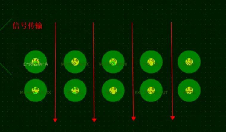
Place the imported footprints inside the outline. Keep signal flow clear, separate analog and digital areas, place core parts first, and leave room for heat. Put the USB connector on the board edge for plugging, put the LED where it can be seen, and keep the resistor next to the LED to shorten the trace.
3.3 Adjust until the placement is workable
Rotate and move parts until crowding and pin conflicts are gone. Leave enough space between parts for routing and soldering.
4. Route the Board — Draw the First Trace and Complete the Nets
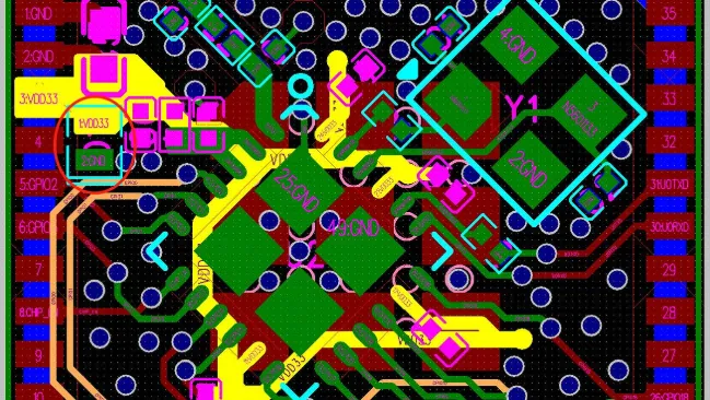
Routing is the core of PCB design: copper traces connect pads according to the schematic nets. This is also the step beginners usually mean by "drawing the first trace."
4.1 Enter routing mode and set basic rules
Turn on routing mode and set rules first: trace width, clearance, and via size. Widen power traces (for example, 1 mm or more) so they can carry current. Ground can be poured later to improve the return path.
4.2 Route manually from pad to pad
Start at one pad, draw the trace, and end on the target pad. That is the first connection. Prefer straight runs, reduce corners, avoid acute angles, and keep signal traces short and direct to limit interference.
4.3 Use layers and vias on a two-layer board
On a two-layer board, top and bottom traces can cross. A via — a plated hole that joins copper on different layers — connects those traces. Keep via size and spacing within the fabricator's limits.
4.4 Pour copper on ground
After routing, pour copper on the ground net. A large grounded copper area improves immunity and helps spread heat.
5. Design Review — Catch Errors Before Fabrication
Do not send the board out as soon as routing looks finished. Run a strict DRC (design rule check) against fabrication limits so shorts, opens, undersized traces, and tight clearances do not reach the factory.
- Confirm every net is connected and none is missing.
- Check trace width, clearance, pad size, and via size against the fabricator's process rules.
- Check silkscreen text and reference designators for clarity, overlap, and offset so assembly and debug stay practical.
Work through the DRC report item by item until there are no violations and the design is manufacturable.
6. Export Files and Send the Board to Fabrication
When design and checks are complete, export the fabrication package and send it to a PCB manufacturer.
6.1 Export Gerber files
Gerber files are the standard fabrication package. They contain the traces, pads, vias, silkscreen, and solder mask on each layer and are what the factory builds from.
6.2 Export the drill file
The drill file lists the location and size of every via and component hole. It is used together with the Gerber files.
6.3 Submit the package and wait for the boards
Zip the Gerber and drill files and send them to the fabricator. Choose laminate (for example FR4), thickness, color, and related options, then place the order. Boards commonly arrive in 3 to 5 days.
7. Beginner Pitfalls to Avoid
- Footprint matching is critical. The schematic symbol and the PCB footprint must correspond one-to-one. A wrong footprint size means the part will not solder. Confirm the package against the component datasheet.
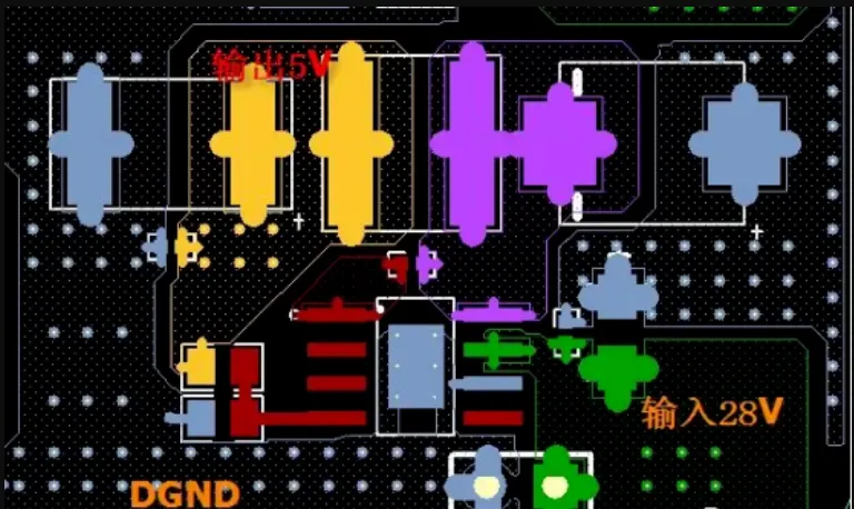
- Handle power and ground first. Widen power traces and pour ground so the supply stays stable and immunity stays high. Many circuit failures start as power problems.
- Keep routing from mixing incompatible signals. Separate high-speed, analog, and digital traces as much as possible to reduce interference and improve reliability.
- Study working examples. Start with simple circuits such as an LED board or a microcontroller minimum system, use open-source projects and practical tutorials, and build experience by doing the work.
Beginner PCB design is not as difficult as it first appears. Follow the flow, start with the first trace, and practice. The skills accumulate, and a board you designed yourself becomes a realistic first result.