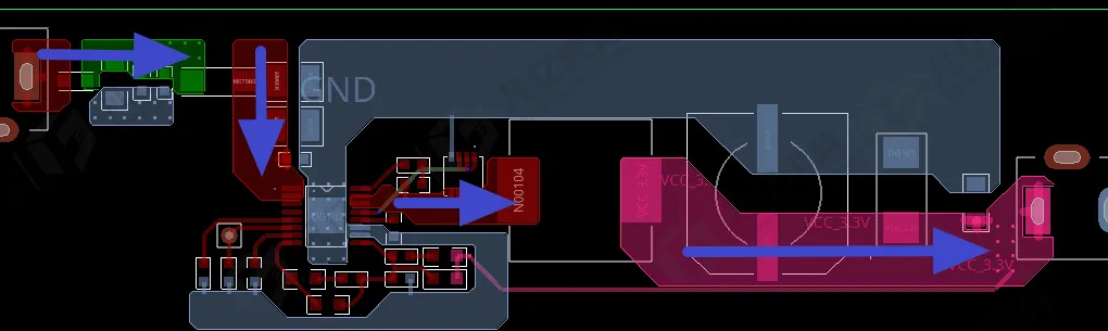
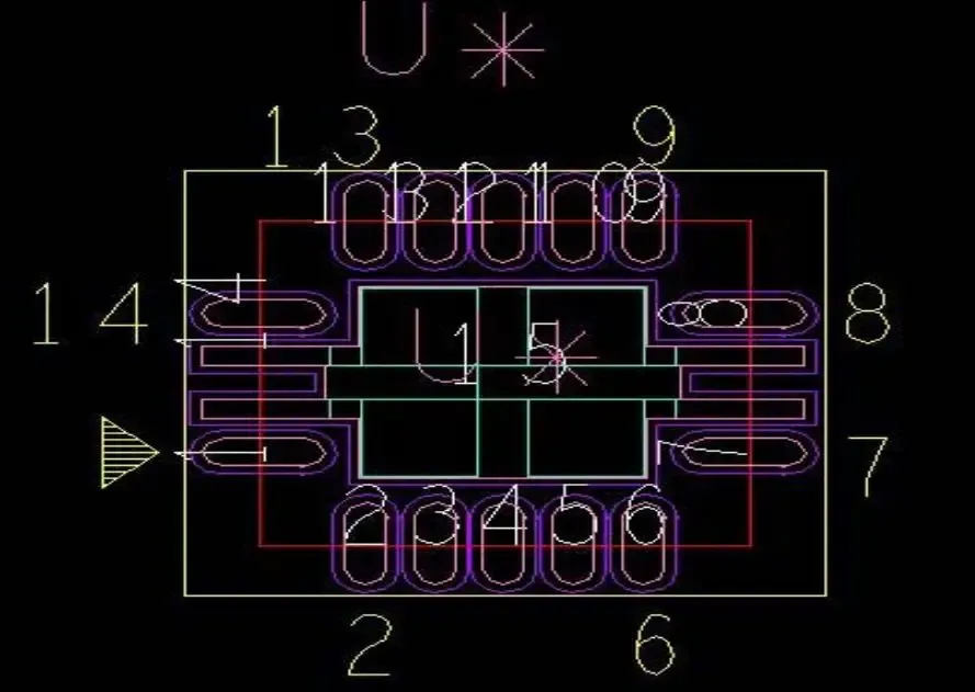
In a dense PCB, a jumper is a small part that still matters. It bridges nets that cannot be routed directly and can rescue a layout. Used badly, it can also take the circuit down. The points below cover jumper types, what they are for, and the details that are easy to miss.
What a Jumper Is
In PCB design, a jumper is a short circuit path made with a heavier conductor or a special connection. It is used when:
- two parts cannot be connected by a normal trace;
- the parts are too far apart;
- a pin numbering error has to be corrected.
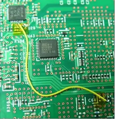
Four Jumper Types
- Wire jumper: simple and direct, but placement must be checked for interference.
- Resistor jumper: can stabilize a signal; the resistance value has to be chosen with care.
- Solder-blob jumper: flexible, but it depends on soldering skill.
- PCB jumper: made through connecting holes; routing flexibility is high.
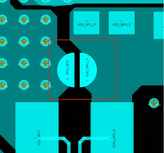
Three Functions
- Complete a difficult net: connect parts that cannot meet on the same layer or in the same area.
- Separate signals: in a high-power circuit, keep paths from coupling into each other.
- Raise reliability: cut the number of open or poorly routed connections so the design stays stable.
Failure Modes
A jumper helps only if these mistakes are avoided:
- a jumper that is too long or coiled → signal attenuation;
- a poor location → interference with other circuits;
- a weak solder joint → an intermittent open;
- missing or incorrect grounding → noise.
Placement and Assembly Rules
- Keep it short and straight. Cut length and avoid loops.
- Stay off sensitive nets, such as high-frequency or analog circuits.
- Inspect the joint. Check solder quality under magnification.
- Verify continuity. Check the net with a multimeter before applying power.
A jumper is small, but it is part of whether the board nets correctly. Used with the rules above, it solves layout problems without adding a new failure.