










Power design is one of the most critical modules in PCB design, and also one of the easiest to get wrong.
Have you run into situations like these?
- The power stage overheats as soon as it is powered up?
- The routing looks clean, but interference is still present?
- The recommended layout in the datasheet is hard to interpret, and it is unclear how the components should be placed?
Power design is not as complicated as it may seem. Once the key principles are in place and the schematic is understood, half of the design work is already done.
This article walks through PCB design techniques for switching power supplies and LDO linear regulators, covering the full flow from placement to copper pour, GND handling, and via arrangement.
Basic Structure of a Switching Power Supply
As shown in the figure, a typical switching power supply module mainly includes the following parts:
- DC-DC converter core: performs power conversion
- Output sensing circuit (R1, R2): samples the output voltage and feeds it back to the comparator
- PWM error-amplifier and drive circuit: controls the output voltage by adjusting the duty cycle
In the figure, the feedback resistors compare the output voltage with the reference voltage Ur. The PWM controller then adjusts the duty cycle to regulate the output.
Key Points of Switching Power Supply PCB Design
1. After device selection, download the datasheet first
The vendor-recommended layout is critical, especially the placement of key components such as input and output capacitors, the inductor, and MOSFETs.
2. Keep the main current path clear and place the core path first
- Center the layout on the switching IC and place components around its pins.
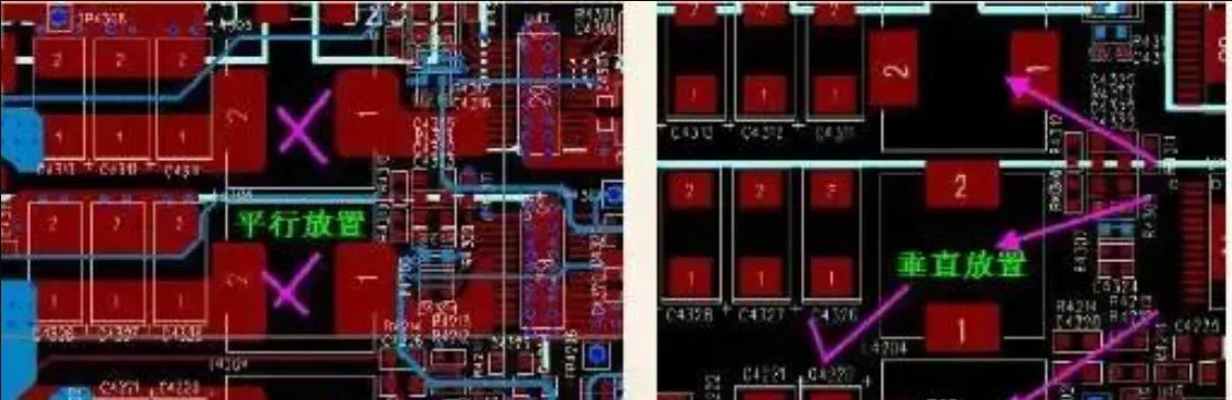
- Do not place the input and output filter capacitors side by side, to avoid coupling input noise into the output.
- Reserve enough space for copper pour and vias.
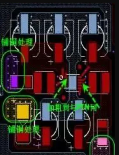
In the figure, the main path is shown with thick traces. Pay attention to current flow and copper distribution.
3. An in-line layout with compact placement works best
- Arrange components neatly along one direction.
- Minimize connection length and the number of vias.
- Place the critical filter capacitors close to the pins, as marked by the red box in the figure. Do not place them arbitrarily.
A compact layout reduces parasitics, lowers EMI, and improves heat dissipation.
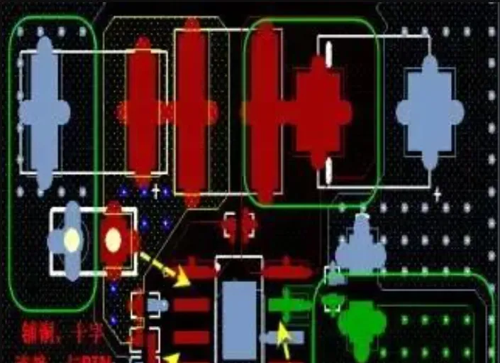
4. High-current routing: use copper pour instead of thin traces wherever possible
- Common ground traces and power input/output traces must be wide or implemented with copper pour.
- Signal interconnect traces should be at least 10 mil wide (most engineers recommend 12-15 mil).
- High-current loops should preferentially run on the top or bottom layer to avoid interrupted current paths.
The figures compare trace widths for different current levels.
5. How to optimize SENSE, GATE, and INTVCC routing
SENSE (sensing) line: use a 0.5 mm trace width, connect it to the far side of the output capacitor, and keep it away from power devices.
GATE drive line: keep it as short and wide as possible, and do not route it next to high-frequency signals.
INTVCC filter capacitor: it must be placed tight against the IC to provide the GATE current supply path.
6. Do not route under the IC or inductor; add thermal vias
- Any IC with a Power Pad needs a solder-mask opening, copper pour, and thermal vias.
- No signal traces should run under the inductor, to prevent magnetic coupling.
- For multiple outputs, place adjacent inductors at right angles to reduce mutual inductance.
7. Copper pour precautions
- Do not connect pads with a fully solid pour. Leave thermal-relief paths for soldering.
- A large copper area must not rely on a single via to connect to ground. Use a via array.
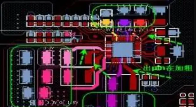
The figure shows common process issues caused by copper pour with no thermal relief, including cold joints, excess solder buildup, and tombstoning.
LDO Linear Regulator Design
What is an LDO? LDO stands for low-dropout regulator.
- It is suitable for low-voltage step-down conversions such as 3.3 V to 1.8 V and 5 V to 3.3 V.
- Advantages: simple structure, fast power-up, low ripple, and a stable output.
- Limitations: it supports step-down only, and the output current generally does not exceed 2 A.
LDO design points, using 5 V to 3.3 V as an example
- Place the input and output capacitors as close as possible to the IC pins. Place the bulk capacitor first (for example, 10 μF), then add the small capacitor (for example, 0.1 μF).
- Keep the main current path short and wide. Use the shortest route possible to avoid extra voltage drop.
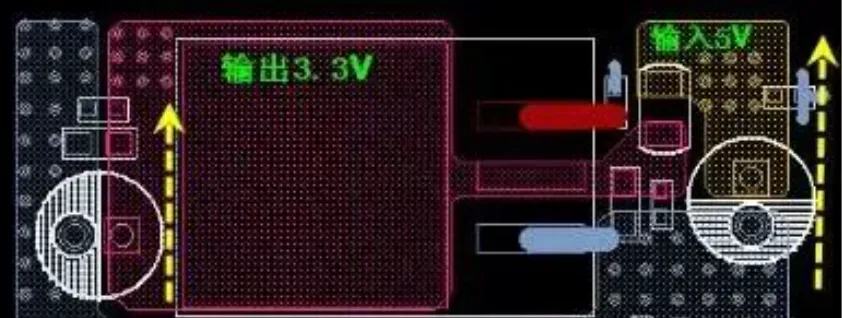
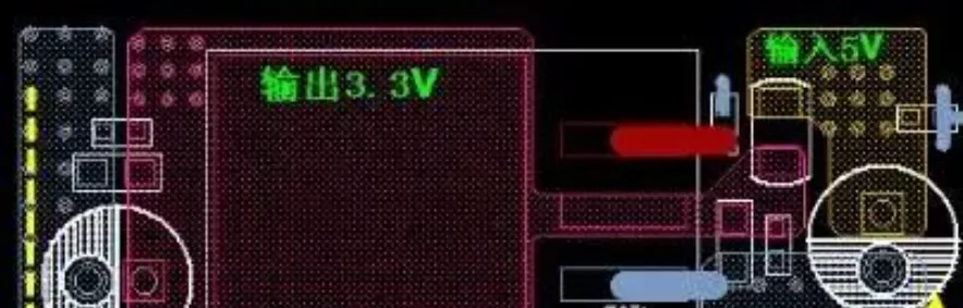
GND main-loop routing
- Connect the GND pin to a large copper area to increase the conductive area.
- Use multiple vias. The via count should follow the input and output trace requirements.
- Connect the input and output grounds together as much as possible to form a closed loop.
The figure indicates the recommended copper width and via arrangement.
Summary
| Design item | Switching power supply | LDO |
|---|---|---|
| Control method | Duty-cycle control | Linear control |
| Input/output placement | In-line layout, close to the IC | Bulk capacitor first, then small capacitor |
| High-current routing | Copper pour or ≥20 mil | Widen the main path |
| GND handling | Single-point grounding plus multiple vias | Large copper pour plus multiple vias |
| Thermal recommendation | Thermal ground vias plus solder-mask opening | An LDO generally does not need extra heat sinking |






