










PCB design is not a matter of stacking circuits on a board. It is a systems-engineering task built on details. An asymmetric pad fanout can tombstone a component. A signal that crosses a plane split can drive EMI out of control across the entire board.
This article skips empty theory and focuses on the practical layout pitfalls that have frustrated countless engineers.
High- and Low-Voltage Signals Must Be Strictly Isolated
Switch-mode power supply boards often place high-voltage power circuitry and low-voltage control circuitry on the same PCB. The high-voltage section (MOSFETs, power inductors) and the control signals (PWM, feedback) must be strictly partitioned so that high-voltage noise cannot couple into the control circuitry, causing false triggering or even catastrophic board failure.
Place the Crystal Oscillator Immediately Next to the MCU
Crystal oscillators have limited drive capability. In high-speed digital systems, placing the crystal far from the main controller can cause:
- Signal attenuation
- Square-wave distortion
- Clock skew and system stalls
Place the crystal directly next to the IC. Keep the traces short, straight, length-matched, and symmetric.
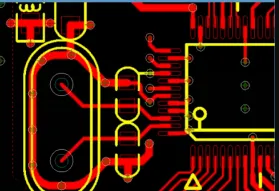
Reuse Modules for Identical Circuit Blocks
On a control board with eight identical input channels and eight identical drivers, circuit blocks repeat. Use the module-reuse function in the PCB design tool so that layout and routing stay consistent and symmetric. That saves time and reduces errors.
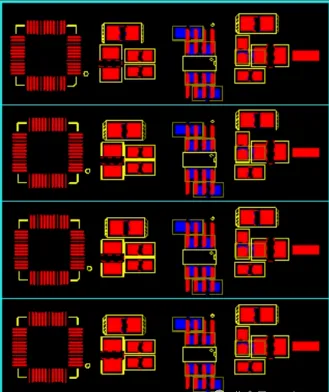
Place Components with the Engineer in Mind
During debug you need room for your hands, probes, and hot-air gun.
- Do not place large parts next to small ones where they block access
- Leave clearance around trimmers, adjustable capacitors, and jumpers
- Avoid overlapping through-hole components
Decoupling Capacitors Must Sit Next to the Power Pins
When power first reaches an IC, voltage droop and spike noise can appear. Decoupling capacitors act as the IC's airbag and absorb those transients.
- Place the capacitor as close as possible to the IC power pin
- Form the smallest possible power–capacitor–ground loop
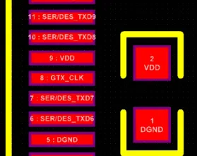
Crossing a Plane Split Is a Signal-Integrity Trap
On a multilayer PCB, if a signal trace leaves one reference plane and crosses into a different region (for example from a GND plane into an unused area), the return path is interrupted. EMI increases and signal quality drops sharply.
High-speed traces in particular must not cross plane splits.
Asymmetric Pad Fanout Causes Rotation and Offset
If traces leave a pad from opposite corners, solder-mask misregistration can rotate or shift the part during reflow and degrade solder quality.
Correct the fanout as follows:
- Keep pad fanout symmetric along the long axis
- Short-axis symmetry further reduces offset
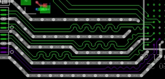
Differential Pairs: Length Matching Comes First
A common misconception is that equal spacing is enough. What actually keeps the pair in sync is equal length.
- Route the pair as a pair
- Prioritize length matching over constant spacing
- Use serpentine tuning where length adjustment is required
High-Frequency Traces Need Ground Guarding or Isolation
Clocks, USB, LVDS, and other high-frequency signals without electromagnetic isolation will:
- Crosstalk into adjacent traces
- Create EMI problems
Recommended approaches:
- Guard with ground (ideally on three sides)
- If space is limited, keep at least 3W spacing
Dense Vias Fracture the Reference Plane
Too many vias, or vias packed too tightly, cut up the GND/VCC reference plane and cause:
- Longer return paths
- Impedance discontinuities
- Scattered noise
Keep via spacing wide enough for a trace to pass between them, and avoid fracturing the ground plane.
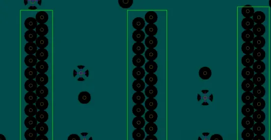
Gold Fingers Require a Complete Solder-Mask Opening
Gold fingers see repeated insertion and extraction. If the solder mask is not fully opened, it will peel over time, raising contact resistance and causing intermittent contact.
Recommended practice:
- Add the opening region in the footprint
- Fully open the solder-mask layer over the gold fingers
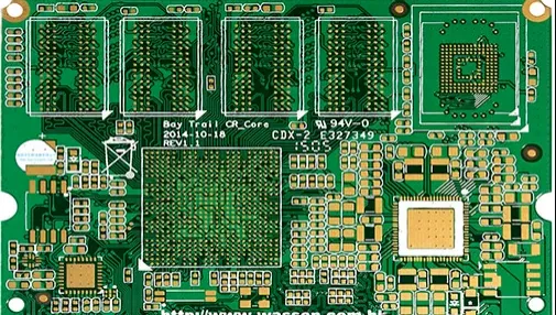
Symmetric Footprints Prevent Tombstoning
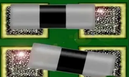
Tombstoning is unbalanced force at the two ends of a part. It is driven mainly by:
- Unequal pad areas
- Inconsistent pad shapes
Design the footprint with fully symmetric pads so the part does not stand up during reflow.

A sophisticated schematic still fails if the layout details are wrong. What looks unimportant can be a fatal trap. A PCB is a structure held up by micrometer-scale details.






