










RF PCB design is not obscure, but many details can still cause a design to fail. Across projects from 2.4 GHz to 28 GHz millimeter-wave, each board reinforces the same point: details decide the result. Recent figures put China's high-frequency, high-speed PCB market at CNY 21.2 billion in 2024, with a projected rise above CNY 30 billion in 2026 and an average annual growth rate of more than 18%. Demand is strong, but the number of engineers who can execute RF PCB design well remains limited.
Why is RF PCB work difficult? The core issues are few: impedance must be controlled accurately, isolation must be handled correctly, thermal design must be planned, and the material must be chosen correctly. Those statements are easy to write. In practice, each one can force several board revisions. At 28 GHz millimeter-wave, ordinary FR-4 can lose as much as 2–3 dB per centimeter, while PTFE can keep loss below 0.3 dB/inch. The difference is large.
Industry data also shows the manufacturing bar. A 5G base-station AAU board often needs 20+ layers, trace-width accuracy of ±0.5 mil (0.0127 mm), and impedance tolerance within ±5%. PTFE costs 3–5 times as much as FR-4, and on 77 GHz automotive radar boards the high-frequency material cost can exceed 60% of the board cost.
1. Layout Practice: Pitfalls Seen on Real Boards
In RF PCB design, layout is the foundation. If the placement is wrong, later routing will not recover the performance. A useful habit is not to start drawing immediately after receiving the schematic. Spend time first on the overall architecture.
1.1 In-Line Layout Is Not Optional
An in-line layout is a basic RF rule. It is simple, but it is often ignored. Route the signal from input to output in order, with as little fold-back and crossing as possible, to reduce interference. On one dual-channel power-amplifier board, the two channels were placed side by side to save area. Intermodulation could not be brought into spec. After the channels were rearranged in line, the specification was met.
1.2 Multi-Channel Designs Need Exact Symmetry
In multi-channel designs, symmetry matters. Approximate symmetry is not enough; placement should be consistent to the millimeter. Component placement, trace length, and via locations on each channel must match so that phase and amplitude stay consistent. On phased-array antennas, a channel-to-channel phase error above 10° reduces beamforming performance significantly.
1.3 Plan the Signal Flow Before Placement
Decide the signal flow before layout starts. Identify which nets are RF, which are control, and which are power. If that is left until routing, paths are often blocked and the placement has to be redone. A simple signal-flow sketch on paper, with the main paths marked, makes placement more predictable.
1.4 Inductor Placement and Orientation Matter
Inductors are critical in RF circuits. Both location and orientation affect performance. High-power inductors need thermal consideration and are better placed near the board edge or next to copper used for heat spreading. Matching inductors should sit close to the related components to reduce parasitic inductance. Orientation is easy to miss: two adjacent inductors with cores placed at right angles reduce mutual coupling.
On one 5G base-station PA board, two matching inductors were placed in parallel. A clear resonance appeared in the 3.5 GHz band and efficiency dropped by more than one percentage point. Rotating one inductor by 90° removed the problem.
1.5 Separate High-Power and Low-Noise Circuits
High-power circuits and low-noise circuits must be separated. The rule is well known and still skipped under schedule pressure. Power amplifiers and switches should be kept far enough from LNAs and mixers. Ground copper or a shielding wall between them helps. A practical spacing is at least 5 mm between the high-power region and the sensitive region. If that is not possible, use a metal shield can.
1.6 Cavity Isolation Is Often Required
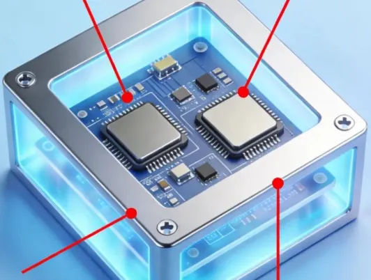
On high-performance RF boards, cavity isolation is close to standard practice. Slots in the PCB or metal shield cans physically separate functional blocks and suppress interference. On current 5G AAU boards, almost every RF channel has its own shield cavity. Cost increases, but the performance gain is real.
1.7 Shield-Cavity Details
A shield cavity is not just a box drawn around a block. Cavity height must be chosen carefully: too low hurts heat dissipation, too high adds cost. Grounding points must be sufficient. A practical rule is one grounding via every λ/10, where λ is the wavelength at the operating frequency. Keep openings as small as possible to limit leakage.
1.8 Optimize Cavity Shape
Cavity shape also affects electromagnetic behavior. Use regular shapes and avoid sharp corners and narrow slots. Sharp corners concentrate electric field and can cause arcing. Slots can act as slot antennas and radiate. Cavity dimensions should also avoid resonances at the operating frequency. Otherwise the cavity can amplify interference instead of suppressing it.
2. Routing Pitfalls
After placement, routing is where experience shows. Boards with acceptable placement still fail when the routing is poor.
2.1 50 Ω Impedance Control Is the Baseline
RF signal traces must be controlled to 50 Ω. There is little room to negotiate this. Impedance is set by trace width, dielectric thickness, and copper thickness. Use an impedance calculator rather than estimating by eye. Many fabricators can hold ±5% impedance control; higher-end processes can reach ±3%. The added cost is often justified.
Impedance control is not only a trace-width problem. Vias, test points, and pads also change impedance. Vias add parasitic inductance and capacitance and create discontinuities. If a via is required, back-drill the unused stub or parallel several smaller vias to reduce the discontinuity.
2.2 Spacing and Vias
Leave enough space between RF traces to limit crosstalk. A common rule is at least three times the trace width, and five times or more at higher frequencies. Do not pack vias densely. Each via is a discontinuity. Prefer surface routing when possible. If a layer change is unavoidable, use back-drilled vias or buried/blind vias.
2.3 Keep Regions Separate
Partition the board into RF, digital, and power regions. Isolate the regions with ground copper and filter the supplies separately. Do not mix digital and RF routing. Harmonics and noise will degrade the RF path. In one extreme case, a clock trace was routed under an RF IC and the noise floor rose by 10 dB.
2.4 Grounding in High-Power Areas
Grounding in high-power areas must be short and wide. Place many vias on PA ground pads—typically 8–12 vias—to keep the ground impedance low. Use thicker ground copper, 2 oz or more, to reduce ground impedance and improve heat spreading.
2.5 Isolate Inputs from Outputs
Keep inputs and outputs isolated to avoid feedback. On boards that integrate transmit and receive functions, separate the TX and RX paths physically, preferably on different layers or with a shielding wall. When input and output were placed too close on one project, oscillation took a week to diagnose.
On one Bluetooth module, transmit power and receive sensitivity stayed out of spec. The PA on the transmit path sat too close to the LNA on the receive path, and the transmit signal coupled into the receiver. Receive sensitivity dropped by 20 dB. Separating the two blocks and adding a shielding wall resolved it.
2.6 Protect Sensitive Signals
Keep sensitive nets such as crystal and reset traces away from RF lines. Their frequency may be low, but the edges are steep and the harmonic content is high enough to disturb RF signals. Wrap them with a continuous ground plane and add a shield can if needed. These nets are often routed on inner layers with ground copper above and below.
2.7 Treat Copper Correctly
Remove floating copper so it cannot act as an antenna. Copper around the RF region should be grounded or removed completely. Avoid long narrow slots in ground copper; at high frequency those slots radiate. Use rounded corners instead of sharp corners, and several small openings instead of one large opening.
2.8 Keep-Out Around On-Board Antennas
For an on-board antenna, there must be no metal, components, or traces under the antenna area. Keep a clearance around the antenna. The keep-out size depends on antenna type and frequency; a common starting point is at least λ/4, where λ is the wavelength at the operating frequency. The dielectric near the antenna should also be uniform. A sudden change in dielectric constant shifts antenna performance.
3. Why These Rules Exist
The points above are more useful when the underlying logic is clear. That logic is what allows the same methods to be applied to new cases.
The central constraint in RF design is that as frequency rises, wavelength shrinks and the structure becomes more sensitive to physical size. At 28 GHz the wavelength is only 10.7 mm. A 10 mm trace is already close to one wavelength, so trace shape and the surrounding dielectric have a large effect. That is why RF layout has to be precise. A small dimensional error produces a large electrical error.
Impedance control exists to reduce reflection. When a signal leaves a transmission line and enters a load, a mismatch reflects part of the energy back toward the source, raises VSWR, and reduces power-transfer efficiency. At 28 GHz, a right-angle bend can add extra capacitance on the order of 20% of the trace width, which is enough to break impedance continuity. RF traces should therefore transition smoothly, without right-angle corners or abrupt width changes.
Isolation exists to prevent crosstalk and oscillation. RF energy couples through space, through the ground return, and through the supply. Harmonics from a high-power amplifier that couple into an LNA input can bury a weak received signal. That is why the PA and LNA must be physically separated and why supplies need independent filtering.
EMC practice on RF boards also follows the 3W rule and the 20H rule: keep an RF trace more than three trace widths away from the adjacent ground-plane edge to reduce edge-field coupling, and inset the power plane by 20H relative to the ground plane, where H is the dielectric thickness, to reduce edge radiation.
Material choice is decisive. Ordinary FR-4 already shows clear loss above 1 GHz, and its dielectric constant can vary by ±10% with frequency. A high-frequency laminate such as Rogers 4350B holds Dk stability within ±0.05 and has a dissipation factor below 0.003. It can cost 5–8 times as much as FR-4, but at high frequency it is often required. Many designs use a hybrid stackup: high-frequency material on the RF layers and FR-4 on the remaining layers, balancing performance and cost.
Thermal design is often underestimated. RF devices are not 100% efficient; most of the unused energy becomes heat. Poor heat spreading raises device temperature, degrades performance, and can destroy the part. On one project, a PA reached 125 °C after five minutes at full power, with 3 dB of gain compression and a 5 percentage-point drop in efficiency. After heat-spreading copper and thermal vias were added, the temperature fell to 85 °C and performance stabilized.
4. Advice for Engineers Starting RF PCB Work
RF PCB design is a skilled task, but it can be learned in stages. Start with simpler boards and accumulate results.
4.1 Start at Lower Frequencies
Do not begin with millimeter-wave. Practice first at 2.4 GHz and 5.8 GHz. Lower frequencies have larger design tolerance and more room for error, so the basic methods are easier to learn. Move higher only after those methods are stable. Starting at terahertz frequencies often produces confusion and little progress.
4.2 Study Proven Layouts
Examine mature designs and look closely at placement, routing, and the handling of details. Open RF board designs are available as references. They may not be usable as-is, but they show how the problems were solved. Early RF work is often spent going through datasheet reference designs many times, including why each trace and via was placed as shown.
4.3 Use Simulation
Simulation is not complete by itself, but skipping it is worse. Tools such as ADS and HFSS can expose problems early. Simulation and measurement will differ, but the trend is usually usable. A practical sequence is a simple transmission-line simulation for impedance and loss before routing, then a full-board EM simulation after routing to look for obvious coupling. The time spent on simulation is often less costly than another respin.
4.4 Iterate in Small Steps
Do not expect a first-pass RF board to meet every specification. Build a version that works, measure it, find the limit, and revise. That loop may run several times, and each pass adds information. One project required five revisions before it met the target. Each revision improved a specific issue, and the final board passed all tests.
4.5 Discuss Designs with Other Engineers
RF work done in isolation is slower. Technical discussion and review by engineers with production experience close gaps that books do not cover. Many RF techniques are found only in measurement and debug. Ongoing discussion of failed measurements remains one of the faster ways to avoid repeating the same error.
Summary
There is no shortcut in RF PCB design. The work is practice, analysis, and review of what failed. Failed boards are part of the path to a board that meets specification.
Industry data indicates that service providers in China with end-to-end high-frequency, high-speed PCB design capability number fewer than 100, and only about 30% can deliver high-speed signal designs above 25 Gbps on a stable basis. That figure shows both the difficulty of the work and the remaining demand for the skill.
Theory is not enough. The test is a board that is laid out, fabricated, and measured. The first time that board works as intended, the result is unambiguous.






