










In embedded hardware design, the DDR power circuit is a core supply block. Its quality directly affects how much of the chip's performance can be used and how stable the product remains over time. As a high-performance processor, the RK3588 places strict requirements on VCC_DDR layout, routing, and component selection. Based on the official design guidelines, this article breaks down the key points of DDR power-circuit design across five areas: copper pour, vias, decoupling capacitors, routing topology, and trace-width rules. The goal is a standardized reference for hardware engineers.
1. VCC_DDR Copper Pour: Size the Path to the Current Demand
Copper pour is the main supply path of the DDR power circuit. It determines current-delivery efficiency and voltage-drop control. Two points need attention:
-
Calculate effective width first
Copper that connects to the RK3588 power pins must meet the chip's maximum current demand. Calculate the effective width in advance with a current-to-width conversion method such as IPC-2221. Insufficient width causes local overheating or voltage loss.
-
Avoid excessive via chopping of the pour
Vias on the pour split the current path. Control via count and placement so every pour path to a CPU power pin stays continuous, with no obvious break in the current channel.
2. Layer-Change Vias and GND Vias: Matching Counts Is What Makes Decoupling Work
When VCC_DDR must change layers, via design should follow the principle of reducing voltage drop and preserving decoupling. The requirements are:
- Power vias: a dense group of 9 or more. When changing layers, place at least nine 0.5 × 0.3 mm power vias. Increasing via count reduces parasitic inductance and resistance, lowers the voltage drop caused by the layer change, and supports power integrity.
- GND vias: match the power-via count. The number of grounding vias on a decoupling capacitor must equal the number of corresponding power vias. Too few GND vias raise the capacitor-loop impedance, weaken noise suppression, and affect DDR signal stability.
3. Decoupling-Capacitor Placement: Place Them Close and Align Them to the Pins
Decoupling capacitors are the noise filters of the DDR supply. Their location determines filtering efficiency. Follow the rules below (the figures make the placement clearer):
-
Capacitors at the core pins: align them on the back side
As shown in Figure 1, decoupling capacitors that sit next to the RK3588 VCC_DDR power pins in the schematic must be placed on the PCB opposite those power pins. That gives the shortest pin-to-capacitor path and absorbs high-frequency noise near the pins.
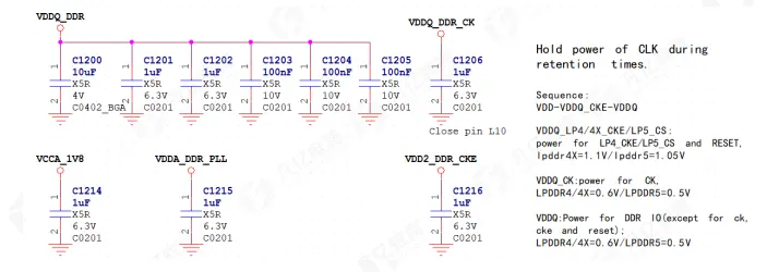
Figure 1 | Decoupling capacitors for the RK3588 VCC_DDR schematic power pins
-
Capacitor GND pads: move them toward the center GND pins
The GND pad of each decoupling capacitor should be as close as possible to the GND pins in the center of the RK3588. That shortens the ground path, lowers ground impedance, and reduces noise coupling into other signals through the ground loop.
-
Remaining capacitors: keep them near the chip
Decoupling capacitors that are not tied to the core pins should follow the placement logic in Figure 2 and be put as close as possible to the RK3588, so every capacitor can suppress noise on the power bus.
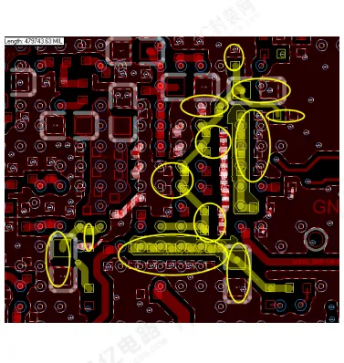
Figure 2 | Decoupling capacitors placed on the back side of the power pins
4. Power-Pin Routing: One Via per Pin and a Hash-Shaped Topology
VCC_DDR power-pin routing on the RK3588 should use one-to-one matching plus a controlled topology. The rules are:
-
One via per pin
Each VCC_DDR power pin must have its own via. Sharing one via among multiple pins causes uneven current sharing and local undervoltage.
-
Top-layer routing: hash-shaped cross connections
As shown in Figure 3, top-layer routing should use a hash-shaped ("#") topology. The cross connections distribute current more evenly. A trace width of 10 mil is recommended to balance current capacity and routing space.
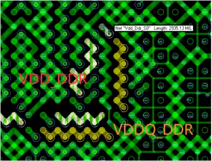
Figure 3 | Hash-shaped connection of VCC_DDR and VDDQ_DDR power pins
-
LPDDR4x mode: use the dedicated connection scheme
When the RK3588 is paired with LPDDR4x memory, follow the routing and via arrangement in Figure 4 for VCC_DDR / VCC0V6_DDR so the supply matches LPDDR4x behavior and the memory stays stable at high frequency.
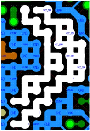
Figure 4 | RK3588 LPDDR4x-mode VCC_DDR / VCC0V6_DDR power-pin routing and vias
5. Trace Width and Copper Pour: Control Them by Region
VCC_DDR width and copper pour should be designed separately for the CPU region and the outer region, while other signal routing is coordinated. The requirements are:
-
Mandatory width rules
- CPU region (around the power pins): width must not be less than 120 mil, to meet the concentrated current at the chip pins.
- Outer region (path from power input to the CPU): width must not be less than 200 mil, to reduce voltage loss over the longer run.
-
Prefer copper pour
Use large-area copper instead of thin traces wherever possible. A larger copper area lowers impedance and voltage drop and improves supply stability.
-
Keep other signals out of the way
Layer-change vias for signals that are not DDR power must be placed to a rule, not at random. That leaves room for the power pour and reduces damage to the ground-plane pour, so the ground plane stays continuous (see Figure 5).
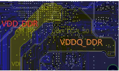
Figure 5 | Copper pour on the RK3588 VCC_DDR and VDDQ_DDR power layers
Summary: The Core Logic of DDR Power-Circuit Design
RK3588 DDR power-circuit design comes down to controlled current delivery, minimum path impedance, and effective noise suppression, so the DDR memory sees a stable, clean supply. The five points above are linked. Copper pour, vias, capacitor placement, and routing topology each have to follow the rules. A small miss can show up as lock-ups, memory errors, or performance variation.
In a real design, hardware engineers should apply the rules to the actual stackup and placement space, and verify the result with simulation tools such as the power-integrity analysis function in Altium Designer, so the finished product is reliable and stable.






