










One question comes up often in PCB design: should the outer layers be poured with copper?
Some designers treat empty board area as wasted space and flood it with GND because it looks more stable. Others argue that, especially on high-speed boards, a careless outer-layer pour can disturb impedance and raise EMI risk.
There is no absolute answer. The professional question is not "pour or not pour." It is:
Does this copper do useful work? Is it reliably grounded? Will it be chopped into fragments? Will it affect signals and soldering?
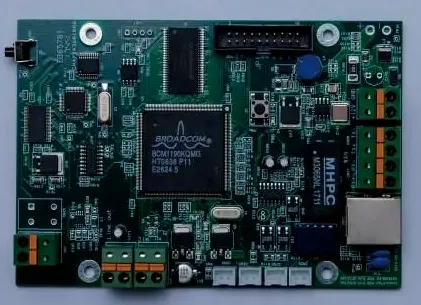
What Does an Outer-Layer Copper Pour Actually Provide?
An outer-layer pour is not meaningless. Used correctly, it can improve overall board performance.
First, it can provide limited shielding. Around low-speed signals, analog circuitry, or other noise-sensitive regions, a well-grounded copper pour can help suppress noise.
Second, copper conducts heat well. Around power regions, power devices, and hot ICs, a controlled pour helps spread heat and reduce local temperature rise.
From a fabrication standpoint, a more even copper distribution also helps reduce warpage caused by uneven heating during reflow.
So the pour itself is not the problem.
The problem is whether the copper you poured is actually useful, or only looks full.
If the copper is well grounded, reasonably continuous, and has a clear return path, it reinforces GND. If traces and parts have chopped it into fragments, it does little good and can create new problems.
The Real Hazard Is Not Skipping the Pour — It Is Creating Copper Slivers
After an outer-layer pour, the board can look covered in red and green copper, as if GND were complete.
Zoom in, and the pour is often sliced by parts, vias, and traces into thin slivers. Some pieces connect to ground at only a single point. Some become isolated copper islands.
That copper is trouble.
It does not form a stable low-impedance return path. It can behave like a small antenna and radiate noise, creating EMI problems.
Long, thin slivers deserve extra attention. Their area may look small, but if the connection is poor and they sit near high-speed signals, clocks, or switching nodes, they can become interferers.
After pouring copper on the surface, clean it up:
- Delete isolated copper islands
- Delete long, thin slivers
- Fix poorly grounded copper
- Remove dead copper with the CAD tools when needed
Do not let a copper pour become a hidden EMI source.
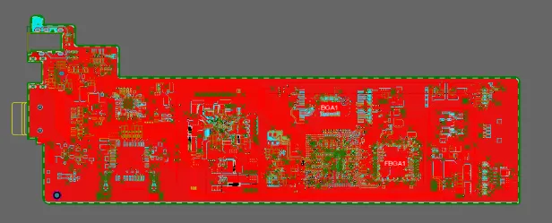
Do Not Solid-Connect Every Pad to a Large Copper Pour
Soldering is another issue that is easy to miss.
If a component pad is tied solidly into a large copper area, the pour pulls heat away during soldering. The pad may not reach reflow temperature, which makes soldering and rework difficult and raises the risk of a cold joint.
For many ordinary SMT parts, pads are therefore not connected solid to a large pour. A cross connection — thermal relief — is used instead.
Thermal relief has three benefits:
- It keeps the pad electrically connected to the pour
- It prevents the large copper area from sinking heat too quickly
- It makes soldering and rework more reliable
High-current pads, power-device pads, and power input/output pads are different. Those locations care more about current-carrying capacity and heat spreading, and often need a stronger copper connection.
Pad connection style cannot be one rule for every part. Small-signal, low-current devices need soldering reliability. High-current, power, and power-path areas need current capacity and thermal performance.
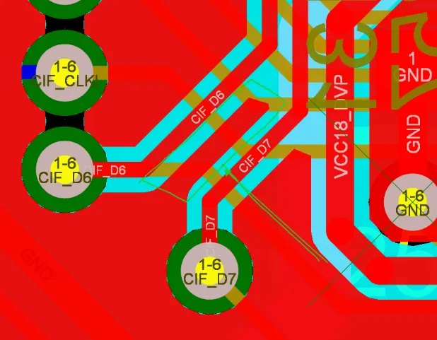
Two-Layer Boards: An Outer-Layer Pour Is Usually Necessary
On a two-layer board, an outer-layer pour is usually worthwhile.
The reason is simple: there is no complete inner ground plane, so signal return paths are less stable than on a multilayer board.
A typical approach is:
- Pour the bottom layer as a continuous GND plane as much as possible
- Place parts, power traces, and signal traces mainly on the top layer
- Stitch top and bottom GND together with ground vias
That makes ground more continuous and improves return paths for some signals.
On ordinary control boards, power boards, interface boards, and small MCU boards, a well-planned pour helps stability and immunity.
Filling every empty area is still not enough. Check three points:
- Is GND continuous?
- Is there a reference ground under the signal?
- Are the top and bottom grounds stitched with enough ground vias?
If the ground under a signal trace is cut, return current must detour. A longer return path increases loop area, noise, and radiation.
On a two-layer board, the goal of the pour is not to fill blank space. It is to keep GND as complete as possible.
Multilayer High-Speed Boards: An Outer-Layer Pour May Not Help Much
On a multilayer high-speed digital board, the situation changes.
Many multilayer stacks already have complete power and ground planes. For high-speed signals, the continuous reference plane under the trace matters more than a copper patch poured beside it.
Take a microstrip. If it sits close to its reference ground plane, return current prefers the path directly under the trace — the lowest impedance and the most direct return.
Nearby outer-layer copper may not reduce crosstalk in a meaningful way. If that copper is too close to a high-speed trace, it can change the characteristic impedance. If the copper is discontinuous, it can create local impedance discontinuities.
That is why high-speed boards should not receive a blind outer-layer pour.
Be especially careful around DDR, MIPI, USB, HDMI, PCIe, Ethernet, and other high-speed regions. Copper can still be poured there, but only after confirming that it will not disturb impedance, fragment the reference, or leave slivers.
If the outer layer is crowded with parts and traces, and the pour would be chopped into fragments, do not force the pour. If the outer layer is relatively open and copper is needed for copper balance, local shielding, or process reasons, keep enough clearance to high-speed traces.
A common engineering rule of thumb is:
Keep the copper pour at least 4W away from high-speed signal traces, where W is the trace width.
For a 4 mil trace, the pour-to-trace spacing should preferably stay no less than 16 mil. Confirm the actual value against the impedance target and the fabricator's process.
Where Copper Pour Helps — and Where to Be Cautious
A simple scene-by-scene check:
1. Two-layer boards: pour copper
Two-layer boards lack a complete reference plane. A pour can improve GND continuity and return paths. The goal is a more complete ground, not a full flood of every gap.
2. Power regions: pour copper with intent
Around power inputs and outputs, high-current paths, and power devices, copper pour lowers impedance, raises current capacity, and helps spreading heat. Keep the power copper short, wide, and direct. Do not create long, thin detours.
3. Analog and high-impedance regions: copper pour can help
Around analog circuits, ADC sampling, power feedback, and high-impedance nodes, a clean grounded pour can provide some shielding. The ground must stay clean. Do not let digital return current cross that region.
4. Multilayer high-speed digital boards: pour with caution
If the inner layers already have complete GND and PWR planes, an outer-layer pour may add little. Handled poorly, it can disturb impedance, create slivers, and raise EMI risk.
A Practical Conclusion
Should you pour copper on the PCB surface? Keep these points in mind:
- On two-layer boards, usually pour, and keep GND continuous.
- In power regions, pour for current capacity and heat spreading.
- In analog and high-impedance regions, pour for shielding and a clean return.
- On multilayer high-speed boards, do not pour blindly. Protect impedance continuity and the integrity of the reference plane.
- Delete isolated islands, thin slivers, and poorly grounded copper.
- An outer-layer pour is not there to make the PCB look full.
Useful copper pour lets current return more directly, heat spread faster, and noise stay lower.
The important skill is not clicking a one-button pour. It is knowing where to pour, where not to pour, and how to inspect the result afterward. That is engineering judgment.






