In circuit design, most of the effort often goes into the schematic and component selection, while PCB placement and routing are finished quickly. The result is frequent fabrication errors or field failures: overheating, interference, and poor solder joints. Many of these issues can be reduced by design choices made before the board is built. The following techniques focus on manufacturability and stable function.
1. Component Placement: Alignment Is Not Enough
Component placement is the base of PCB design. It must follow the circuit and also fit the assembly process. A layout that only looks tidy can still be difficult to solder and assemble.
- Keep similar parts in the same orientation. Place resistors, capacitors, and other like components in one direction so the assembly machine does not keep changing angle. This improves throughput and reduces the chance of incomplete or incorrect joints.
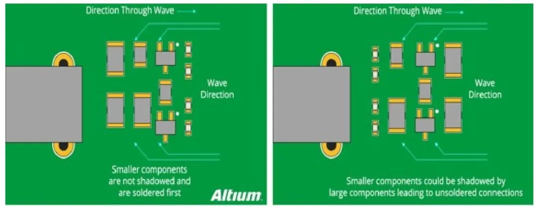
- Do not let large parts shadow small parts. Do not place a small component directly under or behind a large one. During soldering of the large part, the small part can sit in a shadow zone where solder does not wet.
- Group parts by process. Keep SMT parts on the same side of the board when possible, and keep through-hole (TH) parts on the top side. The factory then does not have to flip the board repeatedly, which lowers assembly cost. If SMT and TH parts must be mixed, include the extra process cost in the plan.
2. Routing: Power, Ground, and Signals Each Need a Plan
After placement, route power, ground, and signals. These paths determine circuit stability. Many interference and supply problems start in the routing.
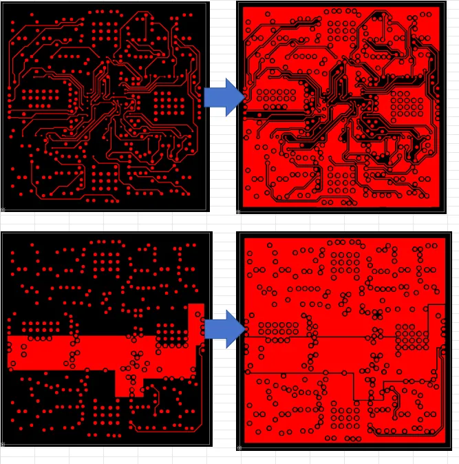
- Place power and ground on inner layers. Keep the power plane and ground plane inside the stackup and centered so the board is less likely to develop multilayer PCB warpage and component location stays more accurate. Use wider traces to feed ICs. Do not daisy-chain the supply from one part to the next, which can make the voltage unstable.
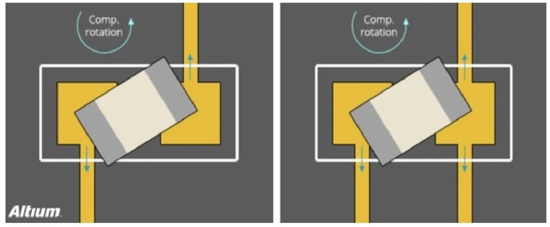
- Keep signal traces short and direct. Use the shortest path between parts and avoid extra bends when a direct connection is possible. If a part must sit in a horizontal orientation, route horizontally first and then turn vertically. Solder flow is then less likely to shift the part. Routing vertically first makes the part more likely to rotate.
- Set width from current. For ordinary low-current digital or analog signals, a 0.010 inch (10 mil) trace is often enough. If current exceeds 0.3 A, increase the width. Higher current needs a wider trace to avoid overheating and trace damage.
3. Isolation: Keep Digital, Analog, and Power Apart
High-voltage, high-current power circuits readily disturb sensitive control or analog circuits. That is a common cause of unstable readings. Isolation reduces the coupling.
- Separate power ground from control ground. Route the power ground and control ground of each supply separately. If they must join, connect them only at the end of the power path, close to that point, so noise is not conducted across the board.
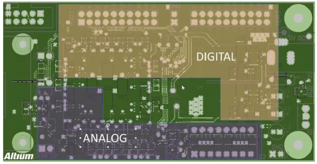
- Keep digital and analog sections isolated. If the board has digital circuits such as a microcontroller and analog circuits such as sensors, place them in separate areas and keep a controlled impedance path on the inner ground plane. Route analog signals only over analog ground. Do not cross digital ground, which increases capacitive coupling.
4. Thermal Design: Heat Can Destroy the Board
Boards that lose performance or fail after a period of use often have poor heat spreading. Power parts in particular lose life when heat builds up.
- Identify the main heat sources. Use the thermal-resistance value in the datasheet. Lower thermal resistance means heat leaves the package more easily. Keep high-power parts such as bipolar transistors and power ICs away from sensitive parts. Add a heat sink or a small fan when needed.
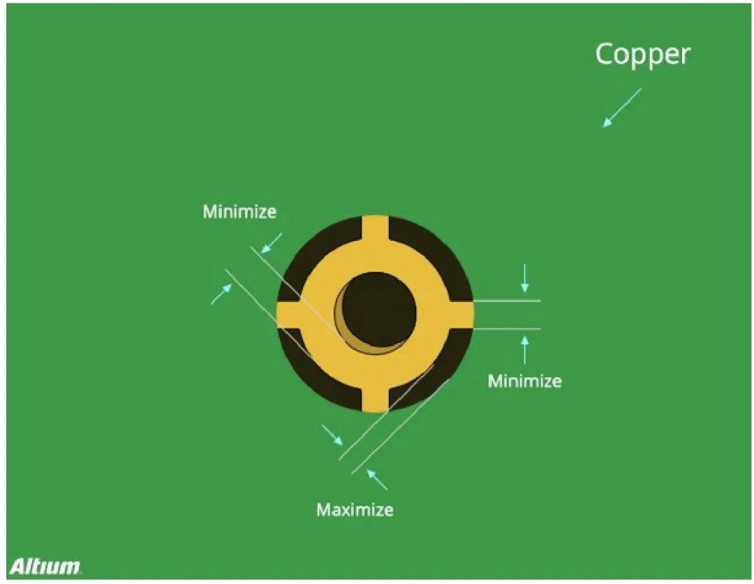
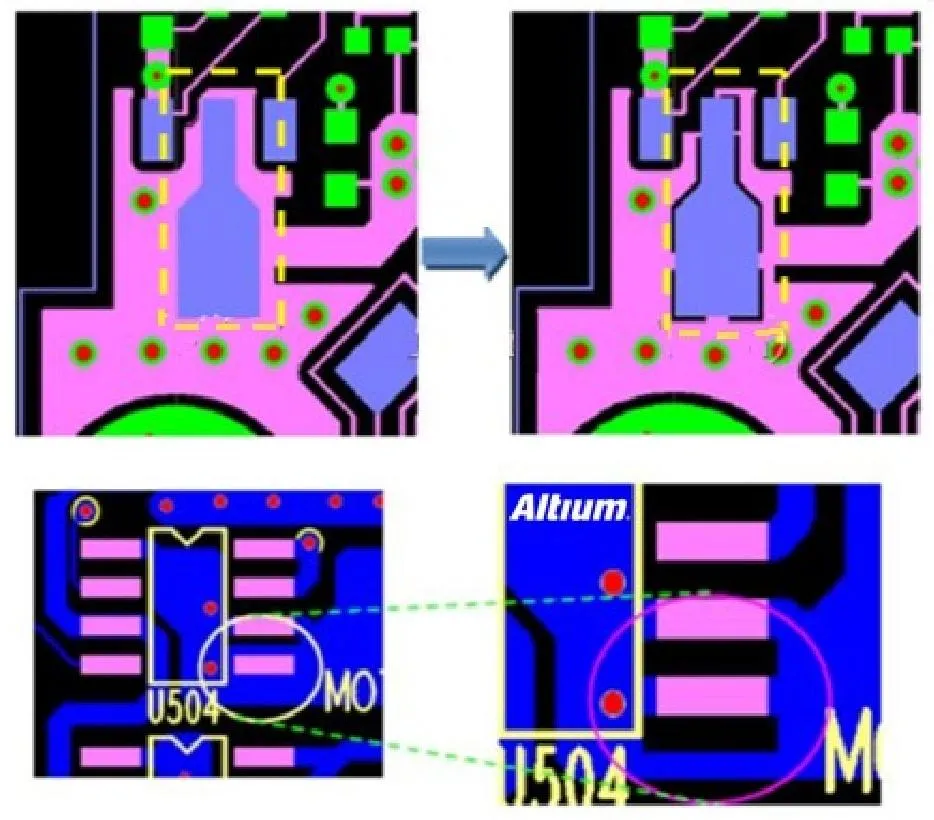
- Use thermal-relief pads. Through-hole parts should use thermal-relief pads. The relief slows heat flow from the pin so the joint can reach soldering temperature and cold joints are less likely. Add teardrops where pads meet traces to strengthen the copper and reduce thermal and mechanical stress.
5. Thermal-Relief Pads: A Direct Fix for Poor Solder Joints
If the function of thermal-relief pads is not understood, the result is voids, incomplete wetting, and cold joints. Changing oven temperature repeatedly does not fix the root cause when the copper connection is wrong.
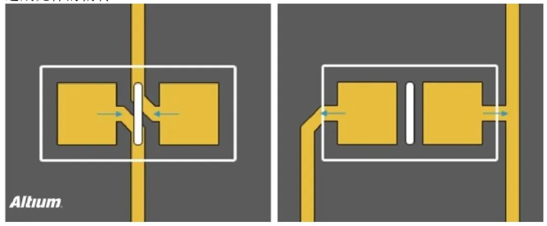
A large power or ground pour heats slowly and spreads heat quickly. If the terminals of a small part, such as an 0402 resistor or capacitor, connect directly to that pour, the pad may never reach solder melting temperature. In hand soldering, heat is also pulled away too fast for a reliable joint.
A thermal-relief pad connects to the large pour through several narrow copper spokes. Electrical continuity is kept, while the heat-spreading area is reduced. During soldering the pad holds temperature long enough for solder to wet the pad.
6. Design Review: Do Not Skip the Last Check
After routing, run a second review. Small errors can scrap the board.
- Run rule checks first. Use electrical rule check (ERC) and design rule check (DRC) in the CAD tool to inspect width, clearance, shorts, and unrouted nets, and confirm the design meets fabrication rules.
- Check signals one by one. Compare each net from schematic to PCB to catch missing or swapped connections. Use the tool's highlighting or masking functions to confirm that the layout matches the schematic.
Summary
PCB design is built around manufacturability and stability. Align components, keep traces short and sized for current, isolate analog from digital, manage heat, use thermal-relief pads, and run a final check. Those six steps remove a large share of common failures.
A first board does not need to be perfect. Practice these basics, then refine them on real projects. A layout that is ready for manufacturing also tends to be more stable and last longer.