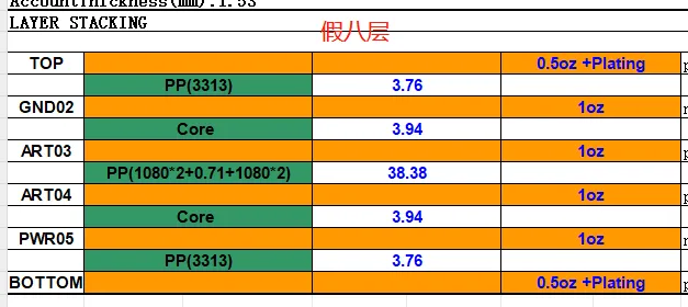
In a multilayer PCB, the stack-up is one of the controlling decisions. A poor stack-up shows up directly in product performance. The rules below are the ones used when the layer order is set.
First, keep each signal layer next to a ground plane. An adjacent ground plane reduces crosstalk and radiated emission between signals. The plane supplies the return path and shields radiation from the signal layer. On high-frequency and high-speed boards, an adjacent ground plane also avoids split-plane crossings. Important signals should therefore be routed on a signal layer that sits next to ground.
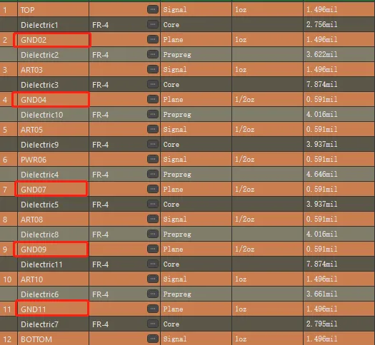
Second, keep the stack-up symmetric. Symmetry affects how much the finished board bows. An asymmetric stack-up warps after fabrication, which then hurts SMT yield and can produce weak or cold solder joints.
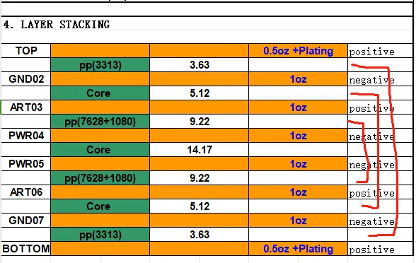
Third, set the layer next to the components as a ground plane. That plane shields the parts and keeps outer-layer signals from crossing a split. Crossing a split means a signal's adjacent reference changes across more than one plane region.
Fourth, place a power plane next to a ground plane whenever possible. The two planes form a planar capacitor and lower the impedance of the power plane.
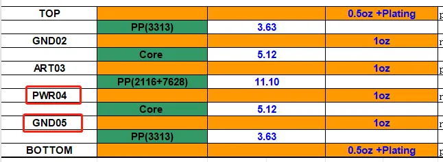
Fifth, avoid two adjacent layers that route in parallel. Crosstalk between parallel routing layers is high and degrades signal quality and board performance. If two routing layers must sit next to each other, run one layer horizontal and the other vertical, or increase the dielectric between them to open the spacing. That is the idea behind the so-called dummy eight-layer stack-up.