










01 | PCB Power Design
The purpose of power design is not merely to convert AC to DC. The power system must deliver correct voltages and currents to circuit components. Low-voltage devices (1.8 V and 1.2 V) remain common, and lower voltages reduce tolerance to power noise.
Power supplies also require current limiting to cap maximum current. Important power-supply parameters include output voltage, maximum current, output voltage ripple, and thermal dissipation at maximum current.
Typical electronic power flows supply voltages in the range from about 1.8 V to 12 V. Common rails include 1.2 V, 1.8 V, 3.3 V, 5 V and 12 V.
In a typical two-stage approach, the first stage converts 230 VAC/110 VAC to an isolated DC rail in the 6–12 V range. The second stage uses a buck switching regulator to step 6–12 V down to 5 V or 3.3 V. LDOs then provide 1.8 V or 1.2 V from the 3.3 V rail.
Before the widespread use of SMPS, transformers stepped down mains to 12 VAC and a bridge rectifier produced a DC of up to roughly 12 × 1.4 = 16.8 VDC; linear regulators then created the required voltages.
Switching regulators have increased conversion efficiency, reduced PCB area, and lowered ripple compared to purely linear systems.
02 | PCB Power Design Considerations
Good PCB layout is essential for power design. Below are seven practical considerations for PCB power design.
1. Appropriate Regulator
Generally, choose between linear regulators and switching regulators. Linear regulators give low-noise outputs but dissipate more heat and may require cooling. Switching regulators are efficient over a wide current range but introduce switching spikes and potential noise on the output.
1) Linear regulators:
- The input voltage must be higher than the output voltage because a voltage drop is required for regulation.
- They produce relatively high power loss and heat, reducing efficiency.
- They are simple, low-cost, and can provide extremely low-noise outputs.
If you select a linear regulator, consider low-dropout (LDO) types and perform thermal analysis before production.
2) Switching regulators:
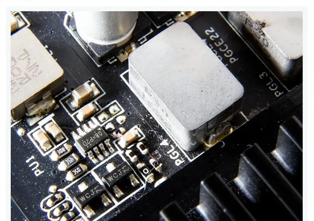
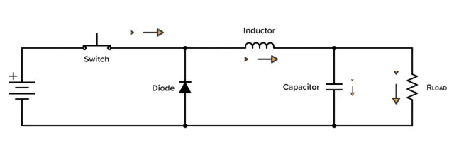
- By temporarily storing energy in inductors and releasing it on switching events, switching regulators convert voltage levels efficiently.
- Fast MOSFET switching allows output regulation by PWM duty-cycle control; efficiency depends on circuit thermal design, where heat dissipation is generally low.
- PWM switching creates output noise or ripple. Switching currents can cause noise coupling into other signals, so switching supplies must be isolated from critical signals.
- They are typically more expensive and require more passive components, but they generate less heat than linear regulators for the same power conversion.
When using switching regulators, plan for electromagnetic compatibility (EMC) mitigation—filtering, minimizing loop area, dedicated ground planes and shielding are common measures to reduce EMI.
2. Thermal Management for the PCB Power System
Power performance depends directly on heat dissipation. Most electronic components generate heat when current flows; emitted heat depends on component power, characteristics and impedance. Choosing the right regulator reduces board heat; switching regulators are typically more efficient because they dissipate less heat.
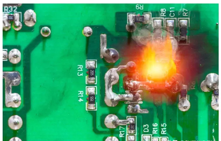
Engineers should consider adequate cooling methods to ensure devices operate within ambient temperature limits.
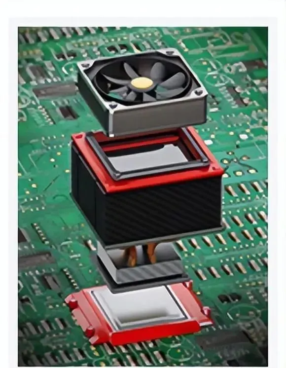
If using a linear regulator, use a heatsink or other cooling approaches; if the device dissipates substantial heat, consider forced-air cooling (fan).
Board-level heat may be non-uniform; high-power components can form local hotspots. Use thermal vias near such components to move heat to internal planes or the opposite side of the board.
3. Dedicated Ground and Power Planes for Better Delivery
Ground and power planes provide low-impedance paths for power delivery. A dedicated ground plane helps distribute power, reduce EMI, minimize crosstalk, and lower voltage drop. Power planes should be dedicated to supplying power to the required board regions.
Engineers should manage different parts of the ground network separately. In multilayer PCBs, one or more layers can be reserved for ground and power. Placing a ground plane between two signal layers reduces interference and crosstalk by surrounding signal traces with return paths.
4. Decoupling and Bypass Capacitors
When power is distributed across the board, active devices cause ground bounce and ringing on power rails. Engineers should place decoupling and bypass capacitors near power pins to meet short transient current demands.
Decoupling reduces impedance between power and ground. Decoupling capacitors act as a local reservoir of charge, supplying instantaneous current to ICs and supporting switching events. All decoupling capacitors must be placed close to IC power pins with their other terminal tied to a low-impedance ground plane. Use short trace connections and nearby ground vias to minimize the series inductance of these connections.
Bypass capacitors shunt high-frequency noise and reduce power-bus fluctuations. Placing bypass capacitors close to devices or ICs, connected between power and ground, compensates for simultaneous switching and variations in power and ground potentials.
5. EMI Filtering
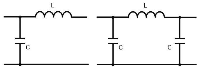
Designers typically require the power supply EMI to remain below specified spectral limits. Use EMI filters at power input points to reduce conducted noise.
6. Frequency Response of the Power Delivery System
When the load changes abruptly (for example, from no load to full load), the output voltage will transiently dip and then recover. In some cases the output may oscillate before stabilizing. If oscillations exceed design limits, adjust output capacitors and compensation components.
For example, for LM7805, a 0.uF capacitor is recommended near the output pin. Sudden unloading of regulators can cause overshoot and oscillation.
To achieve the desired transient response, verify selected components operate within their design limits. AC and DC circuit responses differ and should be considered separately.
7. Power Integrity (PI)
Engineers must ensure power integrity in the power design. Power integrity is the quality of the power delivered to the circuits. It measures how effectively power travels from the source to the load throughout the system, ensuring all circuits receive appropriate power for correct operation.
Low-noise power enhances power integrity. Power-integrity design is essentially managing power-system noise.
These are the seven key points summarized for PCB power design.






