










Engineers who work on high-speed boards have often heard the term "fake 8-layer," also called a pseudo-8-layer stackup. The board is labeled as eight layers, yet it does not provide that many routing layers. The question is whether this is a reduction in construction quality or a controlled compromise. This article explains the structure, when it is useful, and when it should be avoided.
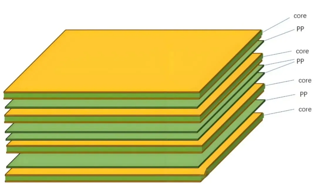
Three Basic Materials in the Stackup
To understand a pseudo-8-layer board, three construction elements need to be clear:
- Core: the rigid copper-clad laminate that carries the board structure and is the main medium for signal layers.

- Prepreg (PP): the bonding material between cores. After lamination and cure, it holds the multilayer stack together.

- Solder mask: often called "green oil," though it is also made in red, blue, black, and other colors. It protects copper from oxidation and reduces the risk of shorts.

True 6-Layer, True 8-Layer, and Pseudo-8-Layer
The two conventional constructions make the difference clearer.
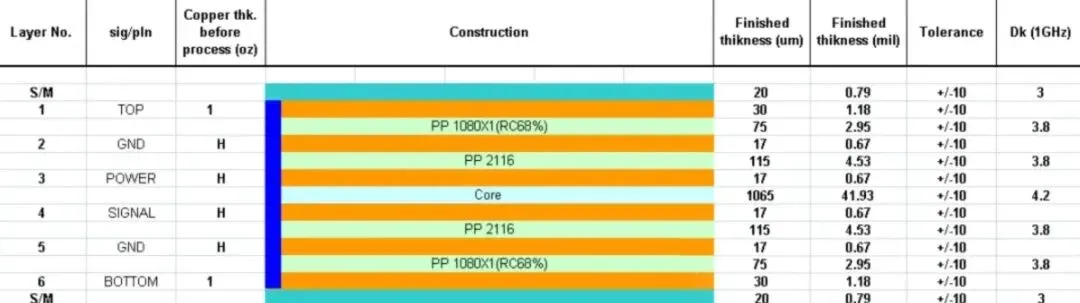
- True 6-layer board: the stack has six layers, but only three of them are available for signal routing in the description used here. The top and bottom layers are often used for components, so remaining routing space is tight in high-density designs. To meet impedance, outer-layer traces may need to be 11 mil wide (about 0.28 mm). That width consumes area and lowers board utilization.
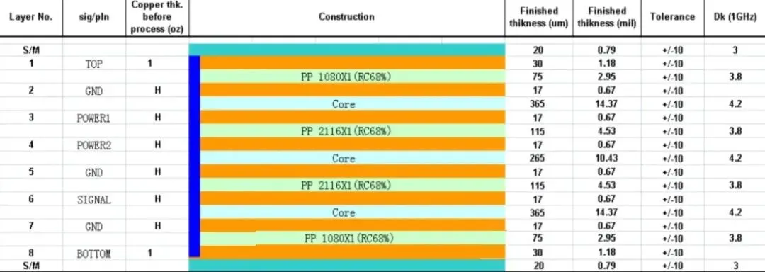
- True 8-layer board: the stack has eight layers, with more routing layers and more space. Signal integrity and immunity are stronger, which suits complex high-speed systems. Cost rises sharply. The step from six layers to eight layers is a clear cost boundary, and many cost-sensitive products cannot absorb it.
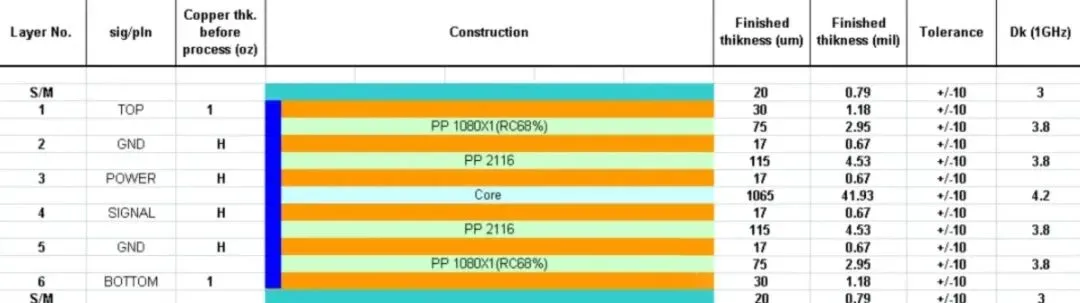
- Pseudo-8-layer board: the method is to thin the cores and outer prepreg of a conventional 6-layer construction, then insert an unclad core in the middle. That extra core does not carry signals. It increases overall board thickness. With this stackup, outer-layer trace width can drop to 5.7 mil (about 0.14 mm), which eases high-density routing.
Advantages and Limits
Advantages: Cost and Routing Density
- Cost: cost is much lower than a true 8-layer board and close to a conventional 6-layer board, which helps when the budget is limited.
- Space: the reduced trace width supports high-density routing without enlarging the board only to fit the traces.
- Interference: the modified stackup can reduce crosstalk between adjacent layers and can be more stable than an ordinary 6-layer board.
Limits: Cases Where It Should Not Be Used
- Performance ceiling: it is still a 6-layer routing structure and does not provide the extra signal layers of a true 8-layer board. In high-frequency applications, signal integrity or EMC may be insufficient.
- Process demand: the unclad core needs special handling, and lamination is more difficult than on a standard board. Not every fabricator can build it.
- Lead time: the process is more complex, and lead time is typically 2–3 days longer than a conventional 6-layer board. Rush orders need extra planning.
When to Use a Pseudo-8-Layer Board Versus a True 8-Layer Board
- Choose a pseudo-8-layer board for 5G equipment, servers, and mid-range routers when impedance control is important, space is limited, the budget is constrained, and the links are not ultra-high-speed.
- Choose a true 8-layer board for high-end servers, ultra-high-speed communications equipment, and complex industrial control systems when signal integrity is the first requirement and cost is not the primary constraint.
A pseudo-8-layer stackup is a cost-and-performance compromise. It does not add routing layers for their own sake. It changes the construction so that impedance-controlled traces can be narrower on a 6-layer routing structure. If a project needs high-density routing without the cost of a true 8-layer board, this option can be evaluated, provided the fabricator can process the unclad-core stackup.






