










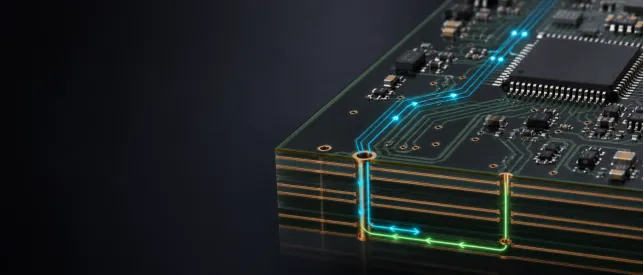
On a high-speed PCB, the first questions are often: was the width calculated, was impedance controlled, was the differential pair length-matched?
Those checks matter. In real projects, many high-speed faults are not a 0.1 mil width error or a few extra millimeters of serpentine. They come from a point that is easier to miss:
The signal went through. The return path did not follow.
A high-speed signal does not work as a single trace. A matching return current always exists. Signal current travels on a surface or inner-layer trace. Return current usually comes back on the adjacent reference plane. The higher the frequency, the more that return current stays directly under the signal trace.
High-speed PCB design is therefore not only how the signal is routed. It is also:
- Is there a continuous reference plane under the signal?
- Does return current have a path when the signal changes layers?
- Is the return path cut when the trace crosses a split, a void, or a power island?
1. Why a Low-Speed Board Works and a High-Speed Board Does Not
On a low-speed design, return current may come back along a lower-impedance path. A detour can still appear to work.
A high-speed edge is fast and rich in high-frequency content. Return current then prefers the path of smallest loop area, which means staying against the reference plane under the signal.
If that plane is continuous, the loop formed by signal current and return current is small. Radiation stays lower and impedance stays more stable.
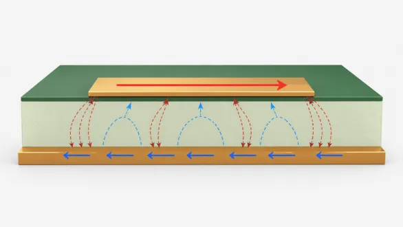
Figure 1 | On a continuous reference plane, return current comes back directly under the signal
If the reference plane is cut, return current must detour. The results are:
- Larger loop area
- An impedance discontinuity
- Higher crosstalk
- Higher EMI risk
- Reflection, overshoot, and ringing on the waveform
- Lower high-speed interface stability
Often the net is connected. The current simply cannot come back.
2. The Most Common Trap: A High-Speed Trace Crossing a Reference-Plane Split
A high-speed net may run over solid GND, then cross a power-plane split, or leave a GND-referenced region for a discontinuous region.
On the PCB view, the trace is continuous and DRC is clean. From the high-speed current view, the reference path is broken.
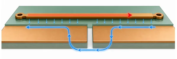
Figure 2 | After a high-speed trace crosses a reference-plane split, the return path is forced to detour
Return current can no longer stay under the signal. It has to find a capacitive coupling path, a ground via, a decoupling capacitor, or some other detour. As the path lengthens, loop area grows, and signal-integrity and EMI problems appear more easily.
Design guidance:
Keep high-speed traces off reference-plane splits.
If a split must be crossed, provide a proper return bridge near the crossing, such as a decoupling capacitor or a ground connection in the right place.
For critical high-speed interfaces, keep the reference plane intact first. Do not cut the plane only to make routing easier.
3. At a Via Layer Change, Do Not Look Only at the Signal Via
High-speed layer changes are common. Many reviews stop at the signal via itself: drill, antipad, stub, and impedance continuity.
Another point still matters:
After the signal changes layers, the reference plane may change too.
A signal on L1 may reference L2 GND. After a via to L4, it may reference L3 or L5. If the planes before and after the change are not the same continuous ground plane, return current must find a new path back.
Without a nearby ground via, that path is forced long.
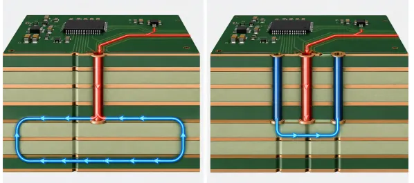
Figure 3 | At a signal-via layer change, a nearby ground via helps the return path switch layers
When a high-speed signal changes layers, place an accompanying ground via next to the signal via-a stitching via or return via-so return current can complete the reference-layer change.
Practical guidance:
- Place a ground via next to a high-speed signal via.
- When a differential pair changes layers, watch the return path of both traces.
- Do not put the ground via too far away, or the return path still grows.
- The higher the frequency and the faster the edge, the more the via-region return path matters.
4. Ground Guarding Is Not a Cure-All. A Continuous Reference Is
Some designers see a high-speed net and immediately guard both sides with ground and stitch vias.
That can be useful, but the purpose should be clear first.
Ground guarding has value when it controls crosstalk, provides shielding, or improves a local return path. If the reference plane under the signal is already discontinuous, a few ground traces beside it do not fully fix the problem.
Priority should be:
- Keep the adjacent reference plane continuous.
- Control trace impedance and spacing.
- Add proper ground vias and shield structures in critical regions.
- Then decide whether ground guarding is still needed.
Do not treat ground guarding as the fix for every high-speed problem.
5. High-Speed PCB Checklist
During a project review, check these items first:
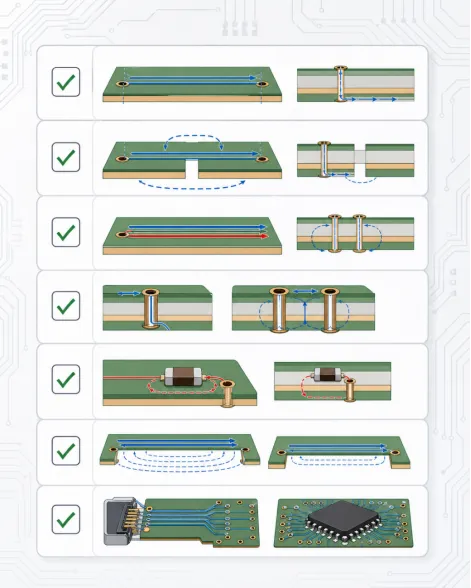
Figure 4 | High-speed PCB return-path review card
- Is there a continuous reference plane under the high-speed trace for the full length?
- Does the high-speed trace cross a GND or POWER split?
- When a differential pair changes layers, is there a proper nearby ground via?
- Does the signal via introduce a clear impedance step or a stub problem?
- Are decoupling capacitors near the high-speed interface close to the power pins and the return path?
- Is there a long detoured return path?
- Are the board edge, high-speed connector, and BGA fan-out regions breaking the reference plane?
If those points are not checked, a clean DRC still leaves high risk.
Closing
High-speed PCB design is not "the net is connected." It is not "impedance was calculated, so the job is done."
A stable high-speed design is judged by a complete current path, not by one trace.
Where the signal goes, the return must come back. Where the signal changes layers, the return must change layers. Where the signal travels, the reference plane must stay with it.
When those questions are settled, many SI, EMI, and late-debug problems are already removed during placement and routing.






