










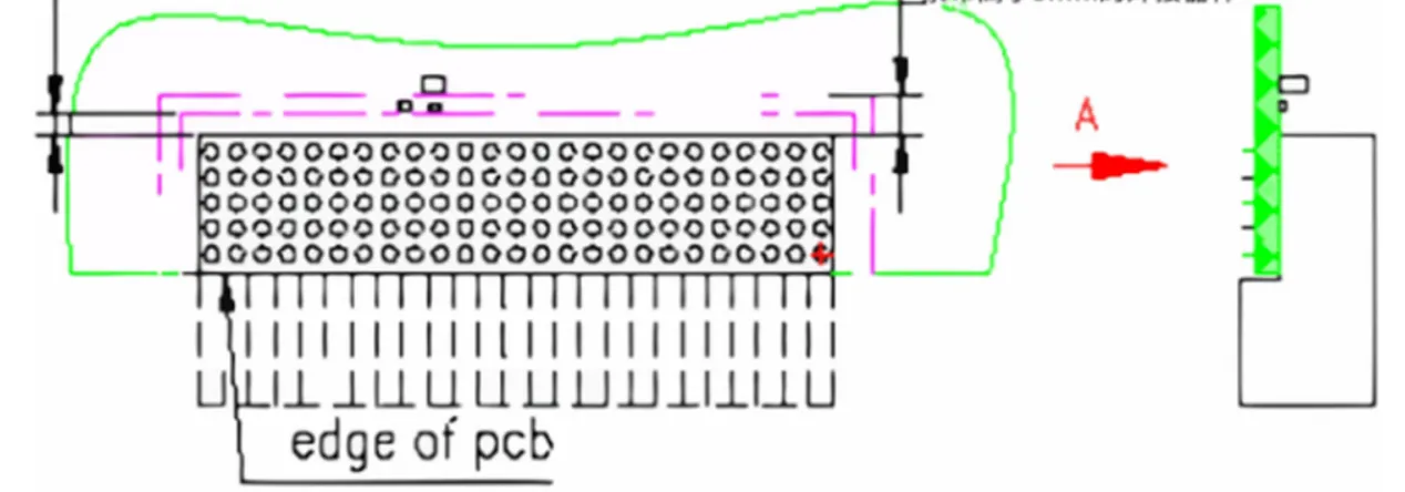
The keepout for a press-fit connector is not a ring drawn around the pads. The connector body, mating shroud, insertion and extraction path, press-fit tooling, and assembly tolerances together sweep a three-dimensional volume. Any component that enters that volume can jam during prototype assembly.
The PCB around the connector may look open, and DRC may report no error, yet the part still will not press down on the assembly line. The problem is usually not insufficient planar spacing. It is that the mating shroud, the insertion direction, and the press-fit motion sweep a three-dimensional volume that the drawing never showed.
The engineering check is direct: a press-fit connector must be reviewed against its 3D motion envelope, not only against 2D component spacing. If the front, back, side, or insertion view is missing, a claimed "1 mm left" may only look safe.
Beyond the Static Outline, There Is Still the Press-Fit Motion
A press-fit connector is not a rectangle sitting above the pads. The pin array passes through the PCB, the connector body occupies space at the board edge or on the board surface, and the press head must apply force from a defined direction. The side-view relationship in the figure shows a height limit that is easy to miss: a low-profile part can still enter the motion zone of the press head or the connector housing.
Drawing only the body outline on the footprint layer leaves out the temporary space used during press-fit, rework, and mating. The footprint library should at least distinguish body outline, assembly keepout, mating keepout, and height limit, instead of packing every purpose into one silkscreen line.
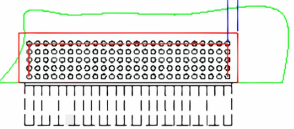
Figure 1 | Connector side view and press-fit direction together form the height keepout
View A Reveals Collisions Invisible from the Side
Seen from the connector end face, the shroud, latch, and guide features on both sides of the pin array are wider than the pad pattern. View A in the source material shows the surrounding keepout relationship and reminds the designer not to treat the pad-array boundary as the connector's maximum material boundary.
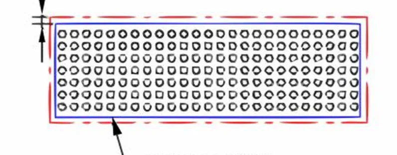
Figure 2 | View A shows keepout remaining outside the pin array
If a tall component is placed next to it, the component body tolerance, placement offset, and connector assembly tilt must also be stacked together. Nominal dimensions that just clear can still interfere in production when worst-case deviations in two directions add up.
The keepout datum should be the maximum mechanical envelope, not the neatest pad edge.
Front and Back Do Not Share the Same Boundary Set
The front of the connector is often constrained by the housing, the plug, and finger access. The back may be constrained by the shroud, pin tails, and the cable bend radius. The two sides have different requirements. One uniform expansion value wastes space on one side and leaves risk on the other.
When the footprint is built, separate mechanical layers can be created for the component side, the solder side, and the mating part. During review, open the corresponding assembly state. Do not ask one 2D silkscreen to carry every mechanical fact.
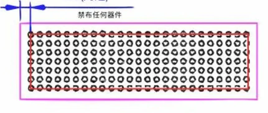
Figure 3 | Datum relationship between the connector front outline and the surrounding keepout
Check the Shroud, Silkscreen, and Keepout Separately
Silkscreen is assembly identification, not the real outline. The shroud outline is the mating-part boundary, not the press-fit tooling boundary. The most reliable check order is to confirm the component body and mating part first, then the press-fit or insertion direction, and finally stack the component and PCB manufacturing tolerances.
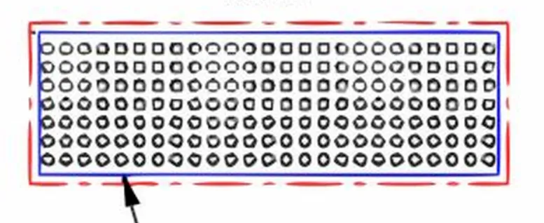
Figure 4 | The back-side shroud outline and the component keepout must be shown independently
When space is truly tight, do not move many parts at once. First pick the object closest to the envelope boundary, add margin in X, Y, and height separately, then recheck with a 3D assembly or mechanical model. That shows which direction is actually limiting the layout.
Different connectors, press-fit equipment, and assembly processes need different margins. The surrounding values in the source material help explain the constraint relationships. They should not be copied without the target part drawing and the factory capability. What must be locked down is the maximum outline, the datum faces, the operating direction, and the source of each tolerance.
Verification after a change should also return to the assembly motion: whether the board can be pressed successfully, whether the plug can fully seat, whether the latch can actuate, and whether rework tools can enter. A 3D model that reports no interference still cannot replace a real assembly check.
The footprint library should also keep version information. After a connector supplier updates the shroud or the recommended hole pattern, an old board that still calls a footprint of the same name may quietly change its mechanical boundary. The review record should state the part number, drawing revision, and mating part used. A generic connector name is not enough.
A board-edge connector also needs the enclosure opening, panel thickness, and PCB locating tolerance placed in the same coordinate system. No interference on the board does not mean the connector will still fully mate after it is installed in the enclosure. Panel offset can put a side load on the plug and, over time, transfer stress into the solder joints and press-fit holes.
If the 3D model is missing, a simplified solid can first be built from the maximum outline and operating envelope, but the data source and unconfirmed dimensions must be marked. Replace and recheck after the supplier model or mechanical drawing arrives. Do not treat a temporary block as the final authority.
Before production, mechanical, PCB, and process engineers can walk through assembly together: start from the incoming orientation and simulate connector locating, press-fit, plug mating, and rework removal. Record the datum face and tool space used at each step. That turns each team's claim that "the spacing is enough" into an object that can be checked.
When the design is frozen, export the keepout envelope to the assembly drawing and the tooling package. Do not leave it only on a mechanical layer inside the PCB editor. Downstream teams need to see it and measure it, or the floor will reinterpret the same boundary from experience.
- Body: verify the maximum material outline of the connector and the mating part.
- Motion: verify the direction of press-fit, insertion, extraction, and rework.
- Tolerance: stack board-hole, placement, enclosure, and component dimensional deviations.
Conclusion
The 1 mm beside a connector is not an isolated number. As long as the keepout is still based on pads or silkscreen, a moved component can still hit the shroud, the press head, or the insertion path.
Put the front, back, side, and motion direction on one checklist. Mechanical problems then do not appear suddenly after the PCB is finished.
Is your current connector keepout drawn from the body outline only, or does it already include the mating part and the press-fit direction?






