Fiducial marks, often called mark points in PCB workflows, are small, intentionally designed features placed on the PCB to support manufacturing and assembly alignment. These reference points allow machine vision systems and operators to accurately locate the board's position and orientation, enabling consistent, repeatable assembly and inspection. Properly designed and placed fiducials improve placement accuracy, shorten setup time, reduce defects, and ultimately increase product reliability.
What Are Fiducial Marks?
A fiducial mark is a high-contrast reference feature used by automated equipment to calibrate positional offsets between the board and the machine's coordinate system. During solder paste printing, pick-and-place, and optical inspection, cameras search for these marks, compute translation and rotation, and compensate for board skew, stretch, or minor panel distortions. By aligning to physical references on the actual PCB, machines avoid accumulating errors that would otherwise come from relying solely on the theoretical board outline or mechanical stops.
In practice, two categories of fiducials are commonly used:
- Global fiducials: Board-level references that define the overall position and rotation of the PCB. These are typically placed near the corners to provide a wide lever arm for precise angular correction.
- Local fiducials: Component- or area-level references located near fine-pitch or critical packages. Local marks allow the machine to refine alignment for a specific region, compensating for localized artwork distortion.
Although many designs implement both, the fundamental purpose is the same: give vision systems a consistent, unambiguous target to lock onto so that every downstream operation proceeds from a known coordinate frame.
How Fiducials Improve Assembly Accuracy
Fiducial marks significantly enhance assembly precision. For surface-mount technology (SMT), global fiducials help the pick-and-place machine identify PCB position and orientation and automatically correct offsets before component placement. Accurate alignment enables the machine to drop components onto pads with tight tolerances, which is particularly critical for fine-pitch ICs, small discrete components, and dense layouts.
Fiducials also benefit manual operations. When rework or hand-placement is required, operators can use fiducials and related board features to quickly understand the intended reference frame, reducing the chance of misplacement. Collectively, these improvements raise placement accuracy, mitigate cumulative tolerances, and improve yields.
Efficiency Gains in Fabrication and Assembly
Beyond accuracy, fiducials streamline processes across the line. In the early stages of board handling and setup, clear fiducial marks allow equipment to quickly locate and register the board, eliminating time-consuming manual measurements and adjustments. Machines can perform automatic alignment checks at each critical step—paste printing, placement, inspection—without operator intervention.
The net effect is shorter setup time, faster job changeovers, and higher line throughput. When alignment is robust and repeatable, less time is spent tuning placement programs or troubleshooting misalignment-related defects. Consistency across runs improves, and the same fiducial scheme can be reused with minimal adjustments when panels or re-spins are processed.
Cost Reduction Through Fewer Errors and Rework
Misalignment causes a cascade of issues: skewed solder paste deposits, off-pad placements, bridging, and insufficient solder joints. By providing reliable alignment points, fiducials reduce these errors and lower scrap and rework rates. The resulting improvements translate directly to cost savings in materials, labor, and line time.
Improved upstream positioning also reduces the risk of downstream issues during solder reflow. When components are placed with correct standoff and pad overlap, thermal profiles produce more consistent wetting and joint formation, cutting down on tombstoning, opens, and other reflow-related defects. Reduced defect density means fewer inspections and repairs, lowering the total cost per unit.
Reliability and Yield Improvements
Accurate and repeatable assembly is a foundation for reliable electronics. Fiducials support consistent solder paste application, precise component placement, and robust inspection alignment. In turn, boards exhibit tighter process control, more stable solder joints, and less variability across production lots. These benefits are crucial for achieving high yields in volume manufacturing and delivering stable, long-lived products to end customers.
Fiducial Geometry and Fabrication
A practical fiducial design example consists of three elements:
- A 1 mm diameter central pad.
- A 2 mm diameter solder mask opening (clearance) around the central pad to expose bare copper.
- An outer conductor ring at 3 mm diameter, which may be circular or polygonal, used as a target feature. The polygonal or circular shape can be chosen based on designer preference.
This geometry yields a high-contrast feature that machine vision can easily detect: the exposed copper pad provides the optical cue, the solder mask clearance ensures clear edges without mask encroachment, and the outer ring can assist detection algorithms that look for specific patterns. While implementations can vary, maintaining a strong contrast between the fiducial and surrounding area is essential for reliable recognition.
In all cases, design the local environment so the camera captures a clean image:
- Keep the area around the fiducial free of silkscreen, text, or other graphics that might confuse edge detection.
- Ensure the solder mask opening fully exposes the copper pad and maintains consistent clearance.
- Avoid placing fiducials inside copper pours or near copper features that reduce contrast.
- Prevent solder from accumulating on the fiducial by ensuring it is not included in a paste layer intended for printing.
Placement Guidelines
Place fiducials on the side of the PCB that contains components. For single-sided assembly, fiducials are typically only required on the component side. If both sides of the board carry components, place marks on each side used in the assembly process.
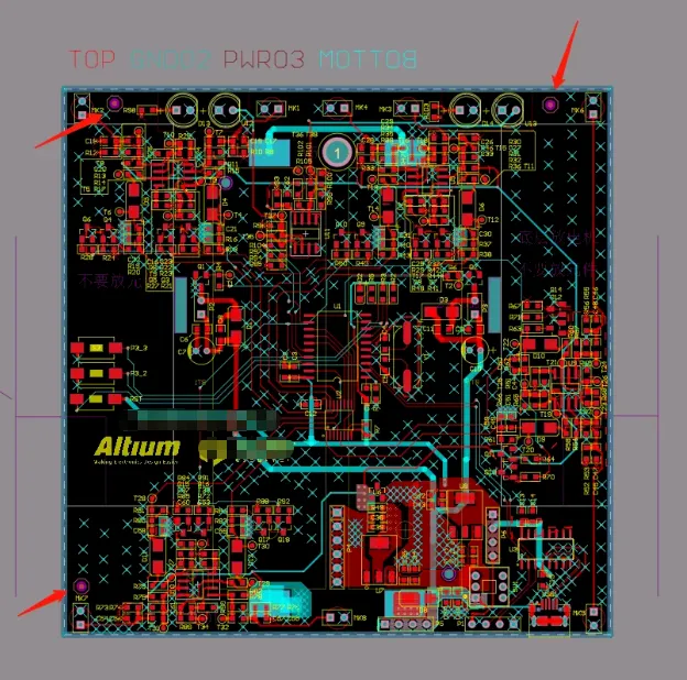
A common practice is to place three global fiducials per side. Locating them near the board edges, typically at the corners, provides a wide baseline for detecting rotation and skew. As an example placement rule, locate the fiducials near the edges, about 3 mm in from the board outline. This spacing provides enough clearance for routing and reduces the risk of mechanical damage while keeping the marks within the camera's field of view during handling and alignment.
Arrange the three fiducials so they are not colinear. A triangular distribution with two marks on one edge and a third on the opposite or adjacent edge is a practical configuration that allows the machine vision system to robustly detect translation, rotation, and subtle scaling or warpage effects.
If a particular device or region requires tighter local alignment, add local fiducials near that area. For example, a fine-pitch component can be accompanied by two local marks positioned diagonally across its placement region to allow the machine to compute a local correction before placing the device. Use local fiducials judiciously to avoid clutter and ensure each one has a clear visual field.
Process Integration Across the SMT Line
Fiducials are used at several stages of the SMT line:
- Solder paste printing: The printer's vision system aligns the stencil to the PCB using global fiducials, ensuring paste apertures overlay the pads accurately.
- Pick-and-place: The placement machine uses fiducials to align its coordinate system to the PCB, then locates component pads and places parts accordingly. Local fiducials are particularly helpful for precision components.
- Inspection: Solder paste inspection (SPI) and automated optical inspection (AOI) systems use fiducials for image registration, allowing precise comparison to expected pad locations and component outlines.
By anchoring each stage to the same physical references, cumulative alignment errors are minimized. This integration reduces defect opportunities and stabilizes the process from printing through placement and inspection, reducing downstream rework and reflow-related issues.
Practical Tips and Common Pitfalls
- Maintain a consistent fiducial design across projects when possible, simplifying machine program reuse and reducing setup confusion.
- Ensure adequate keep-out areas for vision recognition. Crowd-free surroundings matter more than the mark's exact geometry in most cases.
- Avoid placing fiducials too close to mechanical features such as panel rails, mouse bites, or V-grooves, where damage or contamination risks are higher.
- Verify that fiducials are included on the correct layers in the design tool and that they are preserved through fabrication outputs. Mislayered or masked fiducials can compromise alignment.
Example Fiducial and Dimensions
The following image illustrates a fiducial style and dimensional example description: a 1 mm diameter pad, a 2 mm diameter solder mask opening, and a 3 mm diameter outer ring or polygon. The outer shape can be circular or polygonal according to preference.
Summary
Fiducial marks are an essential element of manufacturable PCB design. By providing high-contrast, machine-readable references, they improve placement accuracy, increase manufacturing efficiency, reduce costs associated with misalignment and rework, and enhance overall reliability. A practical approach is to place three global fiducials per assembly side near the corners (about 3 mm in from the board edge) and add local fiducials only where needed for fine-pitch or critical components. Sound geometry, clear surroundings, and consistent implementation ensure that automated equipment can reliably use these marks throughout paste printing, placement, and inspection, delivering stable, repeatable production results.