A phone charger or notebook adapter converts wall-outlet AC into the DC rails a product needs, such as 5 V or 3.3 V. This article covers why that conversion is required, the two common AC-DC methods, a complete circuit block list, an HFC0500 application example, and PCB layout rules.
Why AC Must Be Converted to DC
Everyday products such as phones and routers need DC rails such as 5 V or 3.3 V. Household supply is 220 V AC, so conversion is required.
Generation sites often sit far inland or on the coast. For long-distance transmission, AC can be sent at high voltage and low current to reduce loss. In the city it is stepped down to 220 V AC and then delivered to the home.
Two AC-DC Conversion Methods
1. Line-Frequency Transformer Conversion
The process has three steps:
- A low-frequency transformer sized for 50–60 Hz AC steps high-voltage AC down to low-voltage AC.
- A rectifier converts the low-voltage AC to DC (rectifier methods are shown below).
- Capacitor filtering then reduces DC ripple and smooths the voltage.
2. Switching Conversion
The steps are more detailed:
- A bridge rectifier first converts AC to DC.
- After a capacitor smooths the voltage, a switching device chops the DC.
- A high-frequency transformer steps the voltage down to a square wave.
- A rectifier diode half-wave rectifies that waveform, a capacitor smooths it, and DC is obtained at the output.
Comparison of the Two Methods
Each method has advantages and drawbacks:
- Transformer method: simple circuit, low noise, and low cost, but large size, high weight, high heat, and low efficiency.
- Switching method: small size, low weight, and high efficiency, but a more complex circuit, more high-voltage-rated parts, switching noise, and EMI that is harder to control.
Blocks in a Complete AC-DC Circuit
A practical circuit includes these core blocks:
- Input filter: removes high-frequency noise so the following stages stay stable
- Rectifier bridge: four diodes convert both AC half-cycles to DC
- Filter: capacitors or inductors form a low-pass filter and reduce ripple
- Regulator: a regulator uses feedback to hold the output voltage
- Output protection: protects the load against overcurrent, overvoltage, and short circuit
- Control circuit: includes the switch-mode controller and coordinates the converter
Example: HFC0500 Application Circuit
The HFC0500 circuit below shows how those blocks work in a real design:
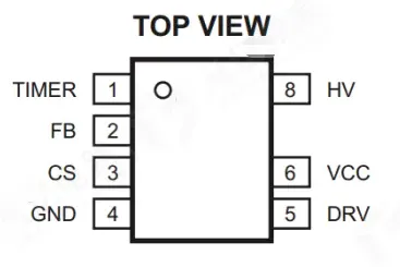
- A fuse provides overcurrent protection, a common-mode inductor rejects common-mode noise, and X-capacitor CX1 reduces differential-mode noise.
- After the bridge rectifier, capacitors provide further filtering, and an RCD snubber protects the switch.
- Pin 5 of the IC outputs the drive signal that chops the switch.
- High-frequency transformer T1 steps the voltage down to a square wave, which diode D6 half-wave rectifies.
- Capacitors C10 and C11 filter the waveform and produce the required output voltage.
- The feedback path uses an optocoupler to isolate the feedback signal and regulate the output.
PCB Layout Rules
For AC-DC PCB design, keep these points:
- Keep the three main loops small: the input loop (C1–T1–Q1–R11/R12/R13–C1), the auxiliary-winding loop (T1–D4–R4–C3–T1), and the output loop (T1–D6–C10–T1). A smaller loop has stronger immunity. Refer to the top and bottom views below.
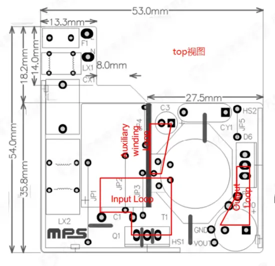
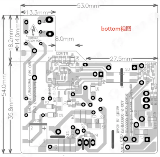
- Split GND: connect input-loop GND to control-circuit GND only at C1.
- Limit high-frequency noise: tie the heatsink of switch Q1 to the main GND plane, and cut away nearby board copper to isolate noise.
- Protect the feedback net: keep it away from power traces and as short as possible.
- Isolate the optocoupler: cut a slot in the board between the two sides of the optocoupler to separate the signals.
AC-DC conversion is the link from the utility supply to the charger. Understanding the conversion method and keeping the power loops short is what makes the circuit both readable and layout-stable.