 00:51
00:51
PCB Stackup
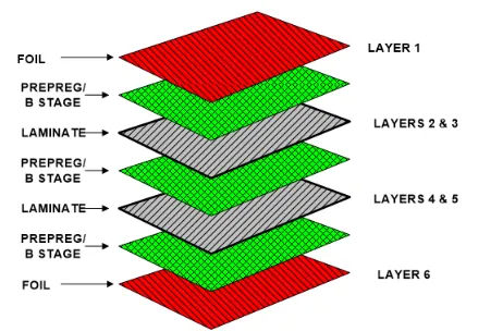
PCB stackup refers to the layered structure of a printed circuit board, encompassing the arrangement of conductive copper layers, insulating substrates, and other materials like prepregs and cores. This configuration is fundamental to the performance, reliability, and manufacturability of modern electronics. For engineers and designers searching for information on PCB stackup, understanding its principles can significantly enhance circuit designs by optimizing signal integrity, managing thermal dissipation, and controlling electromagnetic interference. Whether you are working on high-speed digital circuits, RF applications, or multilayer boards for compact devices, a well-planned stackup ensures impedance matching, reduces crosstalk, and improves overall board durability. In practice, effective PCB stackup design involves selecting the appropriate number of layers—ranging from simple two-layer boards for basic prototypes to complex 20+ layer setups for advanced systems like servers or aerospace equipment. Key best practices include balancing layer symmetry to prevent warping during fabrication, incorporating ground and power planes for stable voltage distribution, and using simulation tools to predict electrical behavior before prototyping. For instance, in high-frequency designs, alternating signal and ground layers can minimize noise, while thicker dielectrics help in high-voltage applications. These strategies not only comply with industry standards such as IPC-2221 but also reduce production costs by avoiding common pitfalls like delamination or signal loss. The articles tagged under PCB Stackup delve into these topics with detailed guides, case studies, and expert tips tailored to various skill levels. From beginner tutorials on standard four-layer configurations to advanced discussions on via structures and material selection, these resources offer practical advice to refine your projects. Browsing through them can provide the insights needed to tackle specific design challenges and stay updated on emerging trends in PCB technology.
Video Guide



Technical Articles
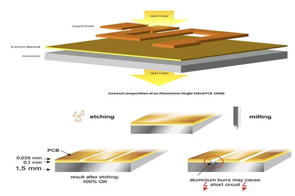
Aluminum PCB Structure Design Guide: Mastering Stackup & Thermal Basics
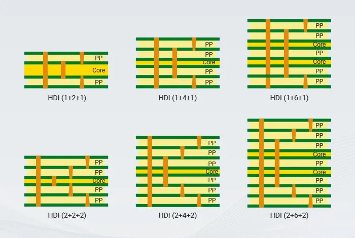
HDI PCB Stack Up Design: Optimizing Layer Count and Signal Routing
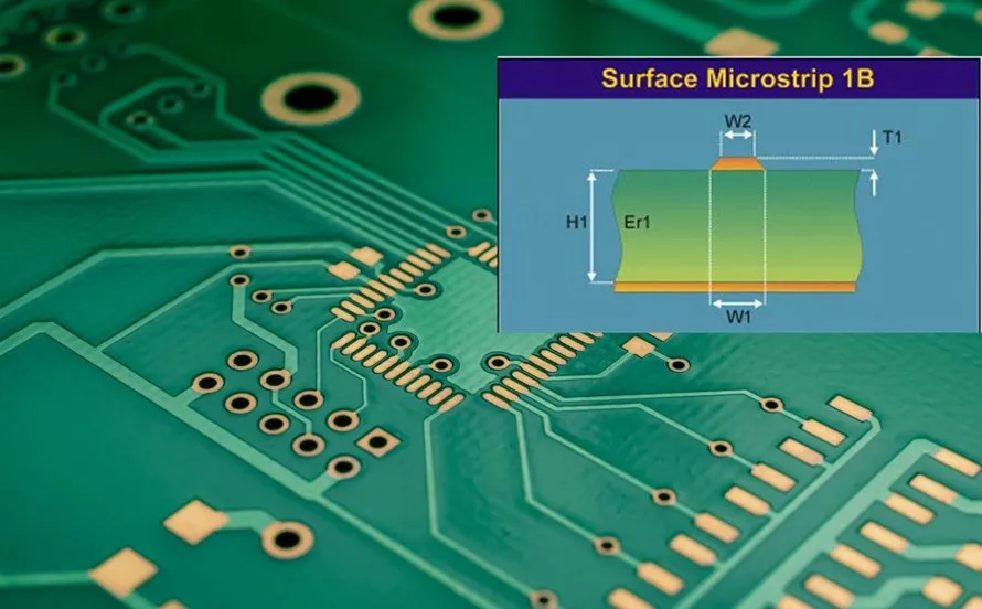
The Ultimate Guide to Designing PTFE PCBs for RF and Microwave Applications
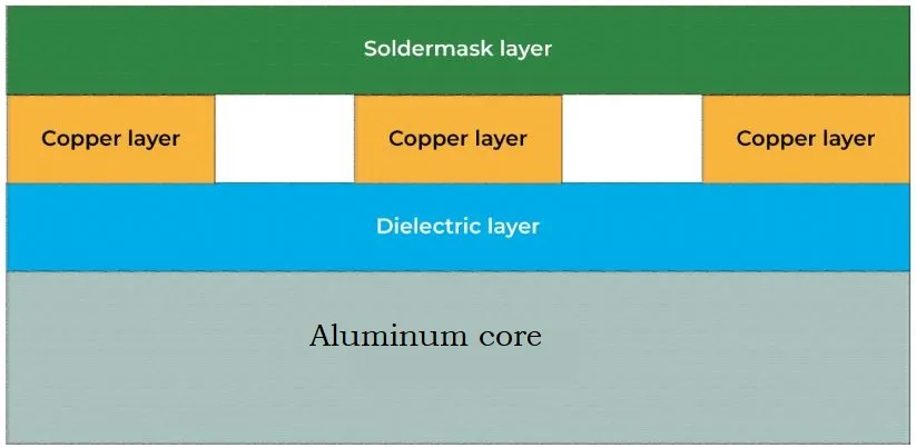
A Beginner's Guide to Metal Core PCB Stackup Design
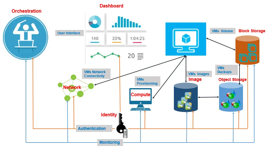
OpenStack Network Models and Use Cases
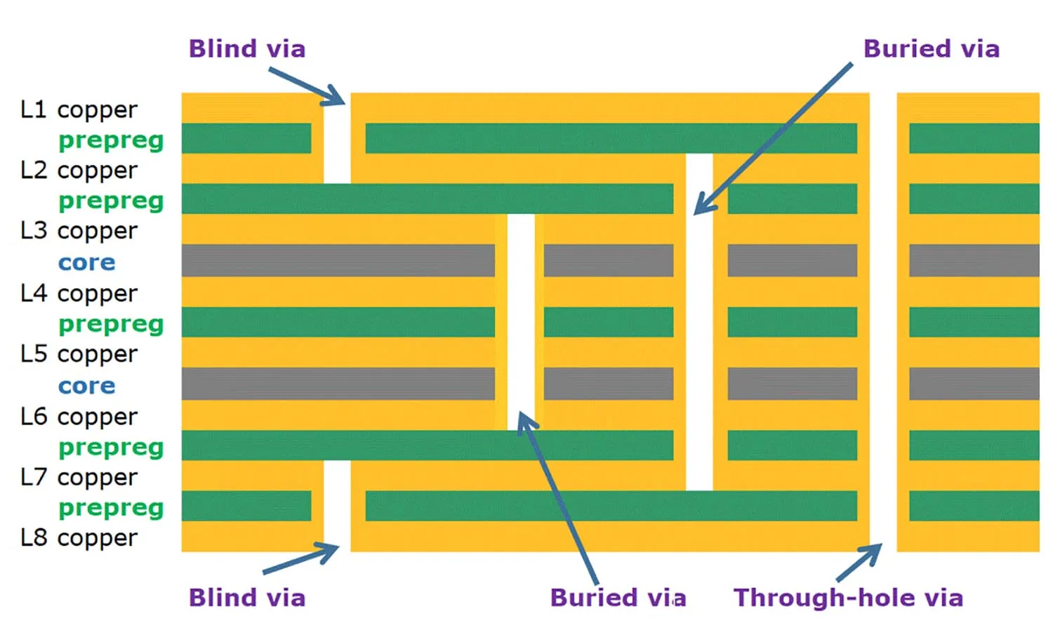
Optimizing PCB Stack Up for High Speed Signals: A Comprehensive Guide

Memory Technologies in New Flagship Smartphones
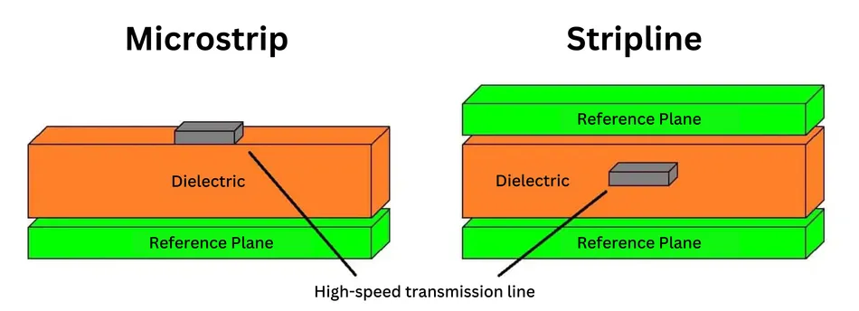
Advanced PCB Impedance Control: Techniques for Minimizing Signal Loss
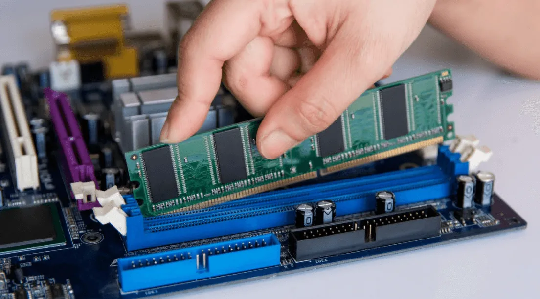
PCB Design Considerations for PC RAM Upgrades: DDR Standards, Cache Integration, and High-Speed Memory Layout
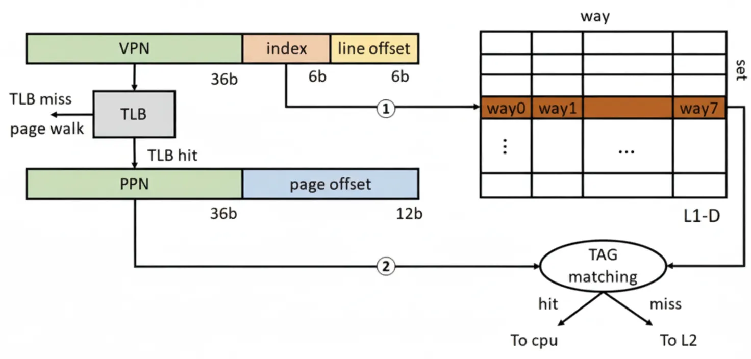
How Cache Size Affects CPU Performance
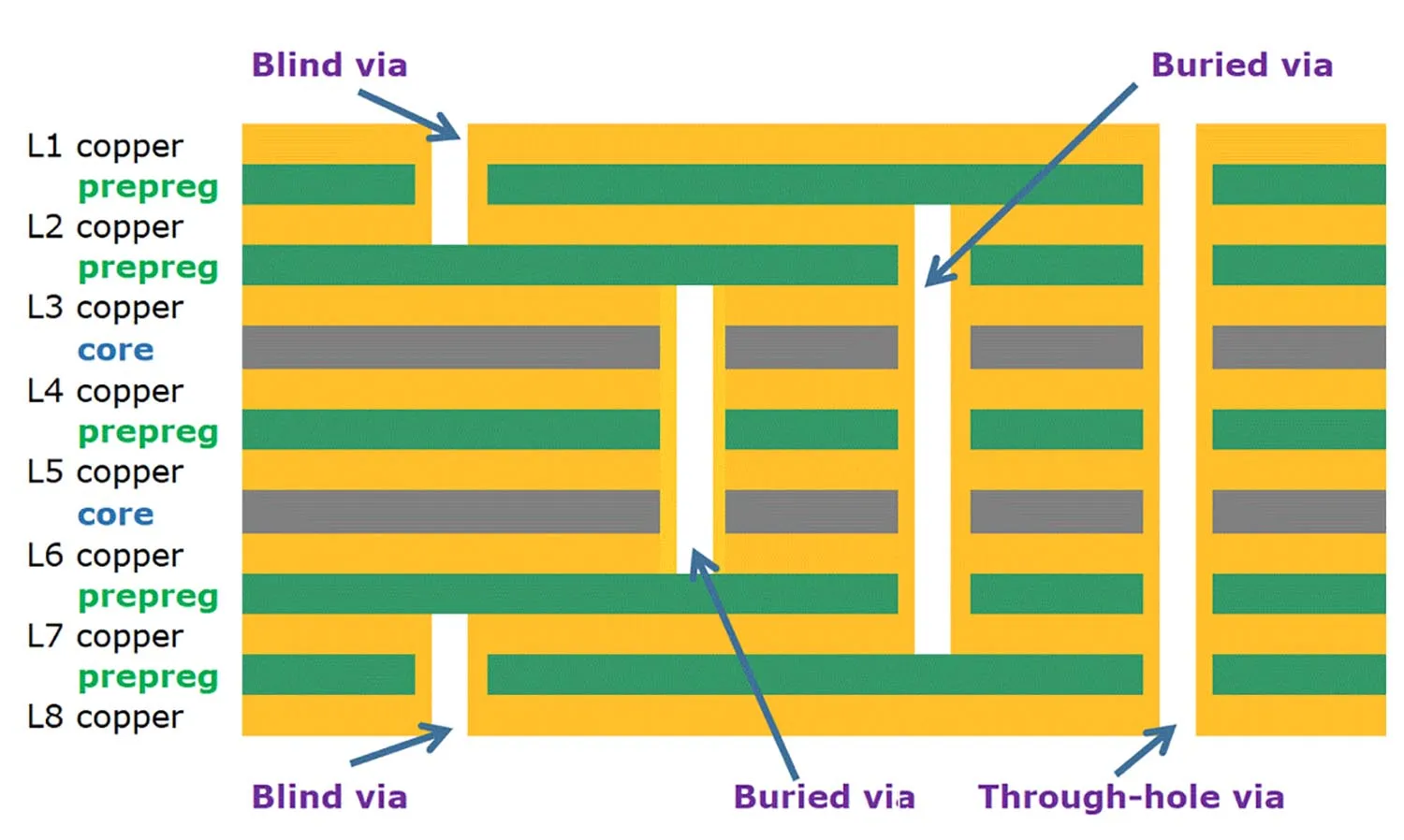
Impedance Controlled PCB Manufacturing: Overcoming Challenges in Design and Fabrication

12 Common Vulnerability Scan Types in Cybersecurity
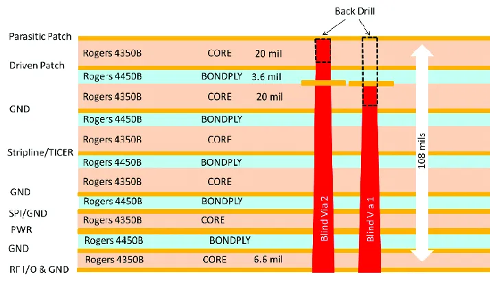
High Layer Count PCB Stackup Design for RF Applications: Minimizing Signal Loss
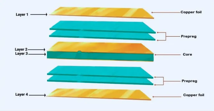
Symmetrical vs. Asymmetrical PCB Stackups: Which Design is Right for Your Project?
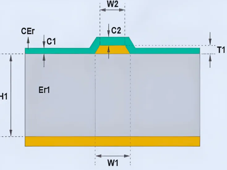
Designing for Signal Integrity: Mastering 50 Ohm PCB Impedance Control
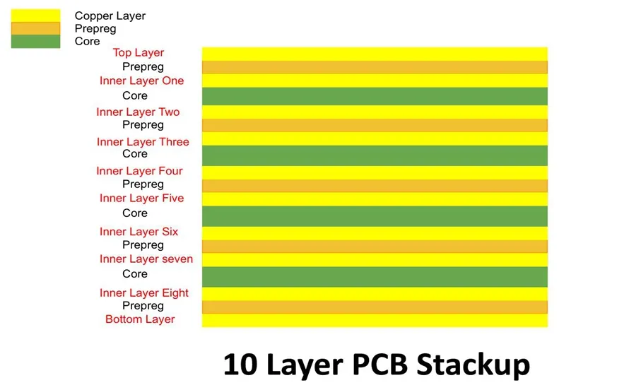
Mastering 10-Layer PCB Stackup: Essential for High-Speed Electronics
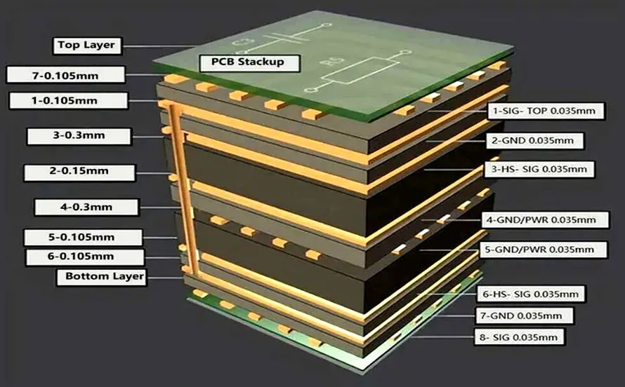
Unleashing PCB Performance: A Guide to Asymmetrical Stackup Design
Optimizing ECU PCB Performance: A Guide to Layer Stackup Design
STM32 FSMC LCD Interface and Timing