Many boards that look clean in KiCad still come back from the fab with assembly problems, excess cost, or failed functional tests. The root cause is rarely a single dramatic error. It is usually a collection of small decisions—messy net names, late design-rule changes, poor placement, or incomplete manufacturing files—that compound into real production risk.
These ten practical tips focus on the decisions that most improve design quality and reduce manufacturing issues when working in KiCad. Each tip links schematic work, layout practice, and the realities of fabrication and assembly so the board that leaves your computer is the board that can actually be built.
Tip 1: Organize Your Schematic Before Layout
A clean schematic is the foundation of a reliable PCB. Disorganized sheets with default net names, floating power pins, and unclear hierarchy make later layout and debugging far harder than necessary.
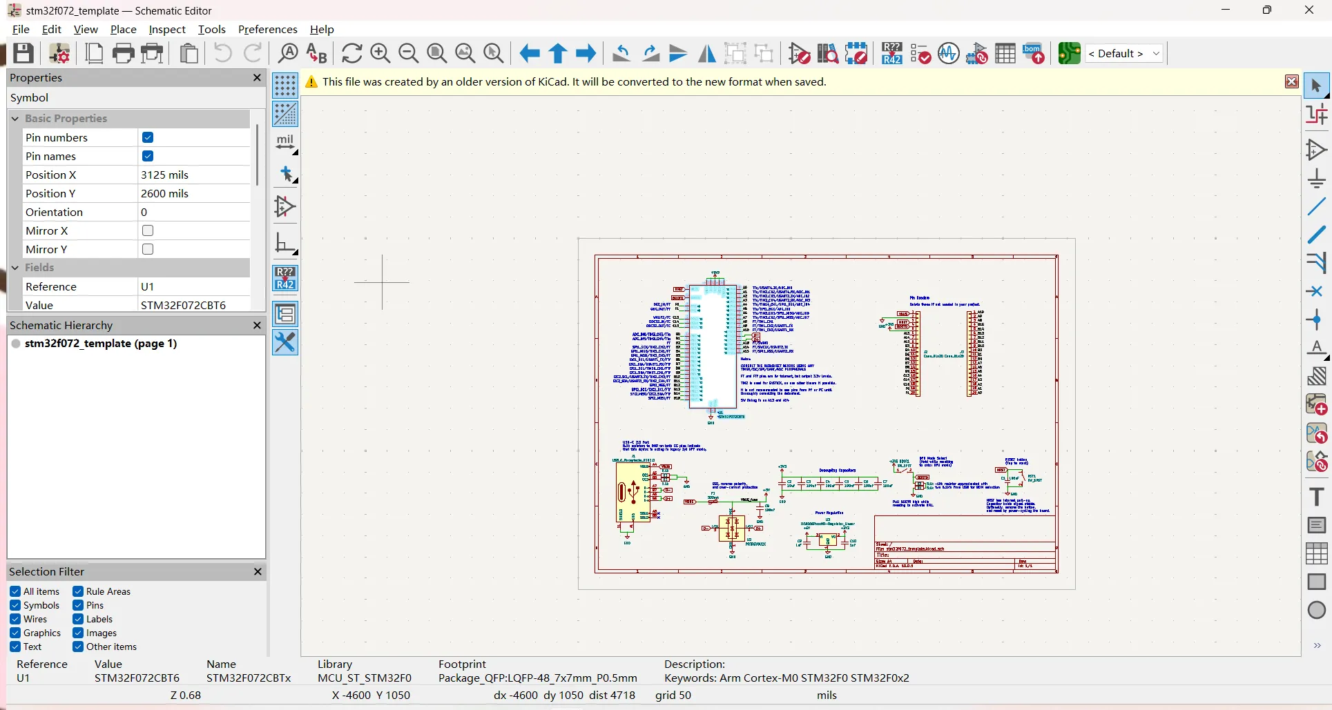
Keep the schematic structured with hierarchical sheets for functional blocks. Use meaningful net names (CLK_25M, VIN_3V3, I2C_SDA) instead of the default Net- labels. Run the Electrical Rules Check (ERC) and clear every error before moving to the board.
Manufacturing perspective: a messy schematic often produces an incomplete or ambiguous BOM. Missing manufacturer part numbers or incorrect values discovered only at assembly force last-minute substitutions or respins.
Tip 2: Use Correct Footprints from the Beginning
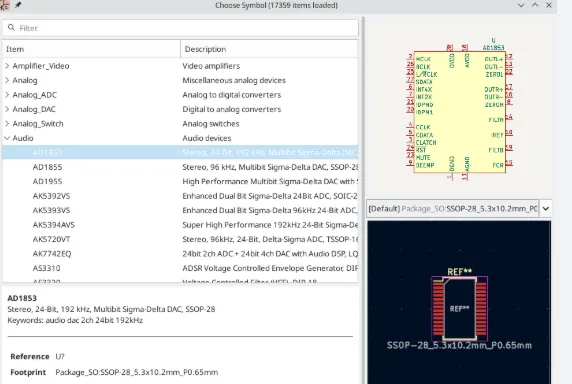
Footprint errors are one of the most expensive mistakes in PCB design. A symbol may be electrically correct while the associated land pattern is wrong for the actual package.
Verify every footprint against the component datasheet land-pattern recommendation before you start placement. Prefer footprints that already include proper courtyard, silkscreen, and solder-mask clearances. When in doubt, create or modify the footprint and save it in a project or company library.
Manufacturing perspective: incorrect pad size, missing thermal vias, or absent polarity marks cause soldering defects and inspection failures. These problems appear only after the board is fabricated and parts are placed.
Tip 3: Define Design Rules Early
Design rules should reflect the manufacturer you intend to use, not KiCad's default values. Set track width, clearance, via size, and annular ring according to the fab's process capabilities before you begin routing.
Create net classes for power, high-speed signals, and general routing. Assign appropriate track widths and clearances to each class. Load these rules into the board so the interactive router and DRC enforce them from the first route.
Manufacturing perspective: rules that are tighter than the fab can reliably produce will cause yield loss or extra charges. Rules that are too loose waste board space and can degrade signal integrity.
Tip 4: Optimize Component Placement
Placement quality determines how difficult routing will be and how well the board performs. Place connectors, crystals, and power components first. Group related circuits together and keep analog and digital sections separated when possible.
Orient similar components in the same direction to simplify assembly and inspection. Leave adequate space for the manufacturer's edge clearances and for any mechanical constraints.
Manufacturing perspective: poor placement forces long tracks, extra vias, and tight clearances that increase fabrication difficulty and reduce assembly yield.
Tip 5: Follow Proper Routing Practices
Route critical nets first—clocks, differential pairs, and high-current paths. Keep signal paths short and avoid unnecessary vias. Use 45-degree angles or arcs instead of 90-degree corners on higher-speed signals.
Let the interactive router respect the net-class rules you defined earlier. After routing, run a visual check for long parallel runs that could cause crosstalk.
Manufacturing perspective: excessive vias raise drill cost and reduce reliability. Tracks that violate minimum width or clearance will be flagged in the fab's DFM review and may require redesign.
Tip 6: Pay Attention to Power and Ground Design
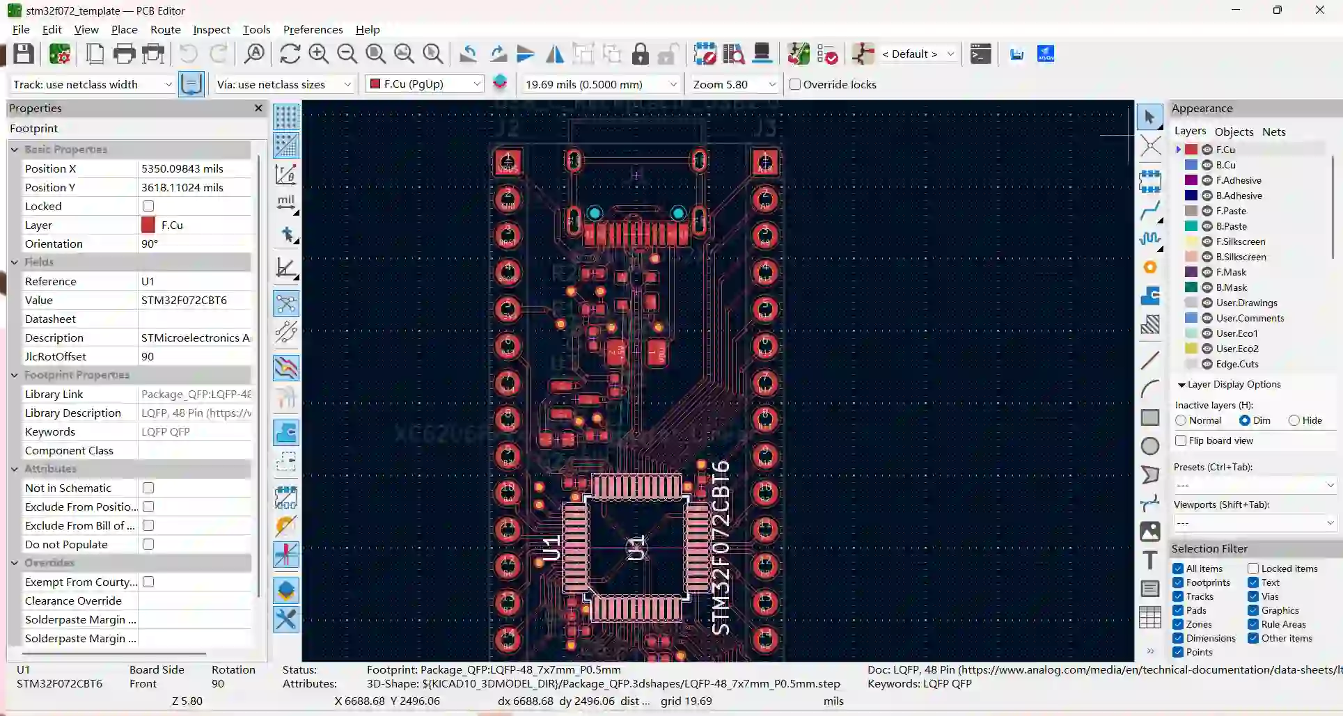
A solid ground plane is one of the simplest ways to improve signal integrity and reduce EMI. Use copper zones for ground and for major power rails. Provide adequate thermal reliefs for through-hole pins unless the current requires solid connections.
Keep return paths short and unbroken under high-speed signals. Place decoupling capacitors as close as possible to the power pins they serve.
Manufacturing perspective: fragmented ground planes or insufficient copper for high-current paths cause voltage drops, heating, and functional failures that only appear under load.
Tip 7: Run ERC and DRC Checks Regularly
Do not wait until the board is finished to run checks. Execute ERC after major schematic changes and DRC after placement and after significant routing sessions. Fix issues while the design is still easy to change.
Treat warnings seriously—many "warnings" become manufacturing or assembly problems later.
Manufacturing perspective: a clean DRC that matches the fabricator's rules dramatically reduces the chance of the board being rejected during the fab's own DFM review.
Tip 8: Consider PCB Manufacturing Requirements
Before finalizing the layout, confirm the manufacturer's capabilities: minimum trace width and spacing, minimum hole size, annular ring, layer stack-up options, and controlled-impedance requirements if needed.
Adjust your design rules and stack-up notes to match those limits. Avoid exotic requirements unless the project truly needs them.
Manufacturing perspective: designing beyond the fab's standard process increases cost and lead time. Designing within their process window improves yield and keeps the price predictable.
Tip 9: Prepare Complete Manufacturing Files
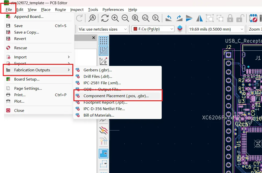
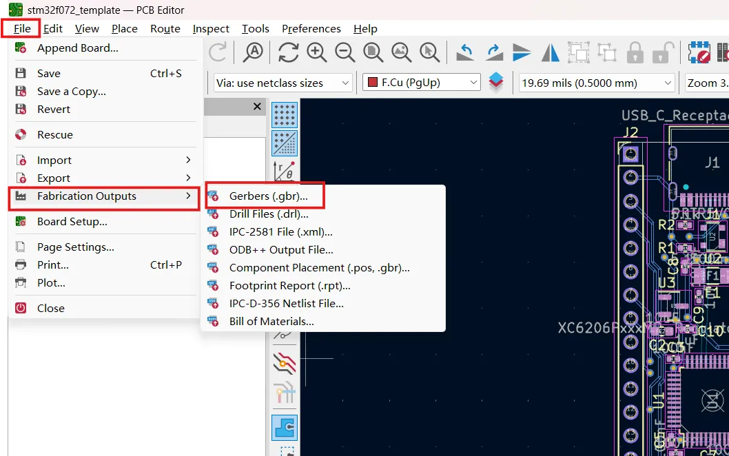
A complete package includes Gerber layers (copper, solder mask, silkscreen, board outline), Excellon drill files, a BOM with manufacturer part numbers, and a pick-and-place (centroid) file.
Use consistent file naming and verify the Gerbers in a free viewer before release. Confirm that the pick-and-place data matches silkscreen polarity marks and reference designators.
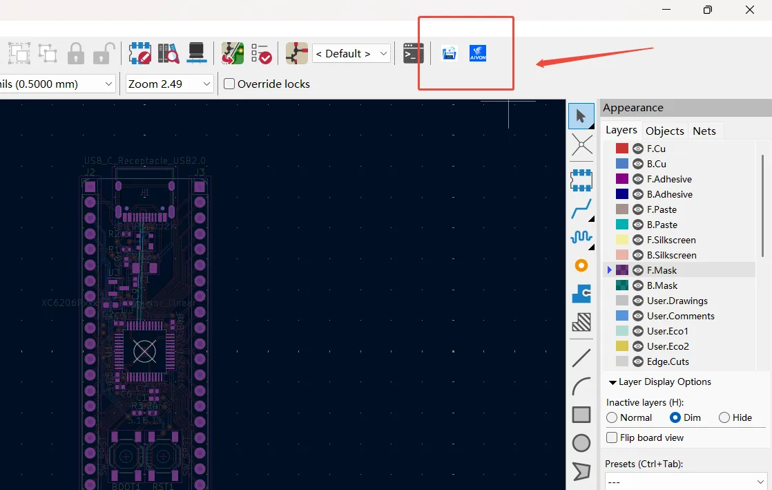
When the files are ready, engineers can use the AIVON KiCad plugin to move directly from the design into quotation and ordering without manually re-uploading every file. This keeps the data consistent and reduces the risk of missing layers.
Tip 10: Communicate with PCB Manufacturers Early
Share stack-up requirements, special materials, impedance targets, or unusual mechanical constraints with the PCB manufacturer while the layout is still in progress. Early confirmation prevents late redesigns.
Ask for a DFM review before committing to production quantities. Most reputable fabricators will flag issues that local DRC cannot catch.
Manufacturing perspective: the cheapest board is the one that does not need a respin. Early communication is the most effective way to avoid production risks.
Applying these ten tips consistently turns KiCad from a drawing tool into a reliable path from schematic to manufacturable board. Clean schematics, correct footprints, early design rules, thoughtful placement and routing, solid power/ground strategy, frequent checks, realistic manufacturing constraints, complete files, and early manufacturer dialogue together produce higher-quality designs with fewer surprises at the fab and assembly house.
FAQ
Q1: What are the most important PCB design tips for KiCad beginners?
A1: Start with a clean, well-named schematic, assign verified footprints early, set design rules to match your manufacturer, and run ERC/DRC frequently. These four habits prevent the majority of costly mistakes.
Q2: How do design rules in KiCad affect PCB manufacturing?
A2: Design rules control track width, clearance, via size, and annular ring. If they are tighter than the fabricator can produce, the board may be rejected or suffer yield loss. Always load the manufacturer's process limits before final routing.
Q3: Why should I run DRC multiple times during a KiCad project?
A3: Running DRC only at the end forces large, late changes. Checking after placement and after major routing sessions catches problems while they are still easy and inexpensive to fix.
Q4: What manufacturing files do I need to send after finishing a KiCad board?
A4: Provide Gerber files for all required layers, Excellon drill files, a BOM with manufacturer part numbers, and a pick-and-place file. Verify the set in a Gerber viewer before submission.
Q5: How can I reduce the risk of PCB assembly problems in KiCad?
A5: Use correct footprints with proper courtyards and polarity marks, keep silkscreen clear of pads, generate accurate centroid data, and confirm component orientation early. These steps directly improve assembly yield.