A board that is perfectly fabricated can still stop at the assembly line if the supporting files are incomplete or incorrect. Missing pick-and-place data, mismatched BOM part numbers, wrong component rotations, or incomplete Gerbers force the assembler to pause, send questions, or make assumptions that often lead to placement errors. Fabrication and assembly require different but related data packages; treating them as the same set of files is a common and costly mistake.
This guide explains exactly how to prepare the full manufacturing package from KiCad for PCB assembly. You will learn what each file is for, how to generate it correctly, which additional documents help the assembler, and the most frequent errors that delay production.
Understanding PCB Assembly File Requirements
PCB fabrication mainly needs copper, mask, silkscreen, and drill data. PCB assembly additionally requires accurate component identity, location, and orientation so that pick-and-place machines and operators can populate the board correctly.
Gerber Files
These define the copper layers, solder mask, silkscreen, and board outline. They are still required for assembly because the assembler uses them to verify pad locations and mask openings against the placement data.
Drill Files
Excellon drill files tell the fabricator (and the assembler for through-hole parts) where every hole is located and whether it is plated or non-plated.
BOM Files
The Bill of Materials lists every component with reference designator, quantity, value, footprint, and—most importantly—manufacturer part number. Without accurate manufacturer part numbers the assembler cannot purchase or kit the correct parts.
Pick-and-Place Files
Also called centroid or XYRS files, these provide the exact X/Y coordinates, rotation, and side (top or bottom) for every surface-mount component. They drive the automated placement machines.
All four file types must be consistent with one another. A part that appears in the BOM but is missing from the pick-and-place file, or a rotation that does not match the silkscreen polarity mark, will cause assembly problems.
Generating Gerber Files in KiCad
Plot Settings
Open File → Plot. Choose Gerber format and the correct output directory. Use the modern KiCad file naming unless the manufacturer specifically requests Protel-style extensions. Enable "Use extended X2 format" only if the assembler or fabricator confirms support.
Layer Selection
Select at least:
- F.Cu / B.Cu (and any internal copper layers)
- F.Mask / B.Mask
- F.SilkS / B.SilkS
- Edge.Cuts
- F.Paste / B.Paste (highly recommended for assembly)
Include any additional layers the manufacturer or assembler has requested (for example, assembly drawings or documentation layers).
Drill File Generation
From the same Plot dialog generate Excellon drill files. Produce separate files for plated and non-plated holes if required. Include a drill map for visual verification. Always open the complete Gerber + drill set in a free Gerber viewer before release.
Manufacturing perspective: incomplete or misnamed Gerber sets are still one of the top reasons for order delays. A five-minute viewer check prevents most of these problems.
Exporting BOM Files
A usable assembly BOM must contain:
- Reference designator
- Quantity
- Value / description
- Footprint
- Manufacturer part number (MPN)
- Optional: supplier part number, tolerance, voltage rating, placement side
In KiCad, use the Schematic Editor → Tools → Generate BOM or a BOM plugin that outputs a clean CSV or Excel file. Fill in every manufacturer part number. Generic descriptions such as "0.1 µF capacitor" are not sufficient for professional assembly.
Practical guidance: freeze the BOM once the design is stable. Late changes to part numbers after the pick-and-place file has been generated create mismatches that the assembler must resolve manually.
Generating Pick-and-Place Files
Component Coordinates
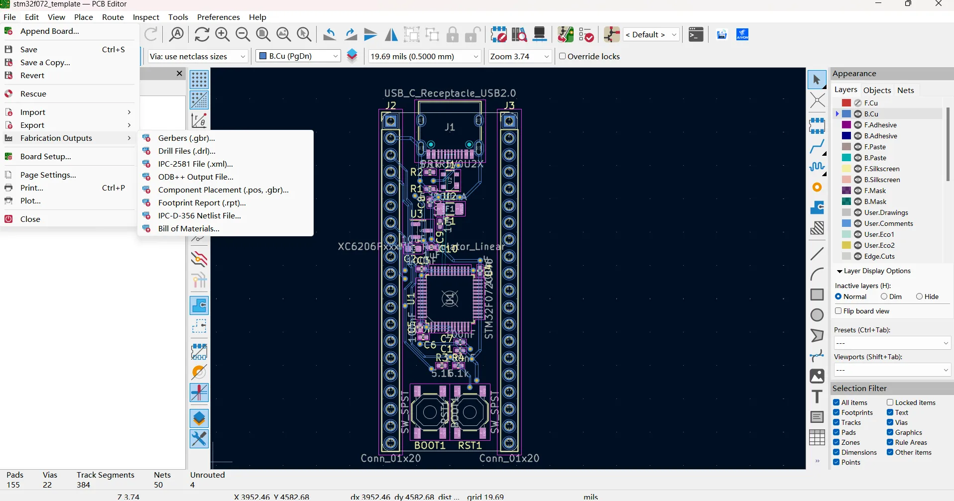
In the PCB Editor go to File → Fabrication Outputs → Component Placement (.pos file) or use the Footprint Position File exporter. The file lists each SMD component's center coordinates relative to the board origin.
Rotation Information
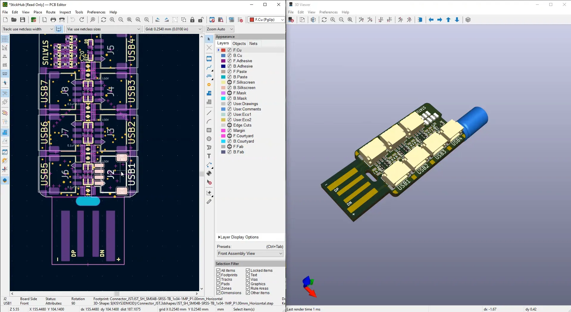
Confirm that the rotation values match the orientation shown on the silkscreen and in the 3D viewer. A 180° or 90° error is one of the most common assembly defects and is often invisible until the board is powered.
Top and Bottom Placement
Generate separate files (or clearly labeled columns) for top and bottom side components. Double-check that through-hole parts intended for manual insertion are either omitted or clearly marked so they are not sent to the pick-and-place machine.
Always cross-check a sample of coordinates and rotations against the board layout before sending the file.
Additional Manufacturing Documents
Assembly Drawings
A simple assembly drawing that shows reference designators, polarity marks, and any special orientation notes helps both automated and manual assembly stations.
PCB Specifications
Include board thickness, material, surface finish, solder-mask color, and any controlled-impedance or special stack-up requirements.
Special Instructions
Note any components that require particular handling (moisture-sensitive devices, tall parts, press-fit connectors, selective soldering, etc.). Clear instructions reduce the chance of process damage.
These extra documents are not always mandatory, but they significantly reduce back-and-forth questions and improve first-pass yield.
Common KiCad Assembly Preparation Mistakes
Missing Files
Omitting the paste layers, the pick-and-place file, or the manufacturer part numbers in the BOM forces the assembler to stop and request data.
Incorrect Rotations
Centroid rotations that do not match the silkscreen polarity marks produce reversed components. Always verify rotations in the 3D viewer and against the silkscreen.
Unmatched Components
Parts present in the BOM but missing from the pick-and-place file (or vice versa) create kitting and placement errors. Keep the schematic, PCB, BOM, and centroid data synchronized.
Other frequent issues include using the wrong board origin, exporting only one side of a double-sided board, and leaving "DNP" (do-not-place) parts in the placement file without clear marking.
When the complete package—Gerbers, drills, BOM with MPNs, pick-and-place data, and any special instructions—is consistent and verified, the board can move smoothly from fabrication into assembly. Engineers can generate these files directly from KiCad and, when ready, submit them for production. Using a workflow that preserves data integrity from the KiCad project through to the manufacturer reduces the risk of file-related delays and assembly defects.
Preparing accurate Gerber, BOM, and pick-and-place files is the final design responsibility before the board enters physical production. A short, disciplined export and verification process prevents the majority of assembly-line interruptions and helps ensure the finished boards match the design intent.
FAQ
Q1: What files do I need from KiCad for PCB assembly?
A1: You need Gerber files (including paste layers), Excellon drill files, a BOM with manufacturer part numbers, and a pick-and-place (centroid) file that includes coordinates, rotations, and top/bottom side information.
Q2: How do I generate a pick-and-place file in KiCad?
A2: In the PCB Editor go to File → Fabrication Outputs → Component Placement. Export the .pos or CSV file, then verify that coordinates and rotations match the silkscreen and 3D view for both top and bottom sides.
Q3: Why must the BOM include manufacturer part numbers?
A3: Generic descriptions are not enough for professional assembly. The assembler needs exact manufacturer part numbers to purchase, kit, and place the correct components. Missing MPNs cause delays or incorrect parts.
Q4: What is the most common mistake when preparing KiCad files for assembly?
A4: Incorrect component rotations in the pick-and-place file and mismatches between the BOM and the placement data. Both are prevented by cross-checking the centroid file against the silkscreen and keeping all files synchronized.
Q5: Should I include solder-paste layers in the Gerber set for assembly?
A5: Yes. Solder-paste (F.Paste / B.Paste) layers are used to create the stencil. Omitting them forces the assembler to generate paste data manually, which increases the chance of aperture errors.