Engineers frequently need to move designs between tools or recover older projects. A schematic started in Eagle, a board received from a collaborator using Altium, or a mechanical outline supplied as DXF must enter KiCad cleanly. Equally important is generating manufacturing files that fabricators can use without clarification. Incomplete imports or poorly configured exports create missing footprints, incorrect layers, and delayed production.
This article explains practical import and export workflows in KiCad, how to migrate from other EDA tools, and the most common problems that appear during the process. The goal is reliable data movement from design to manufacturing.
Why Importing and Exporting Matters in PCB Workflows
Modern PCB projects rarely stay inside a single tool for their entire life. Teams switch software, reuse legacy designs, incorporate mechanical data, or hand files to manufacturers. KiCad's open formats and built-in importers reduce friction, but success still depends on understanding what transfers cleanly and what requires manual cleanup. Correct export settings ensure the Gerber, drill, and documentation package matches the finished board.
Importing Designs into KiCad
Importing Existing KiCad Projects
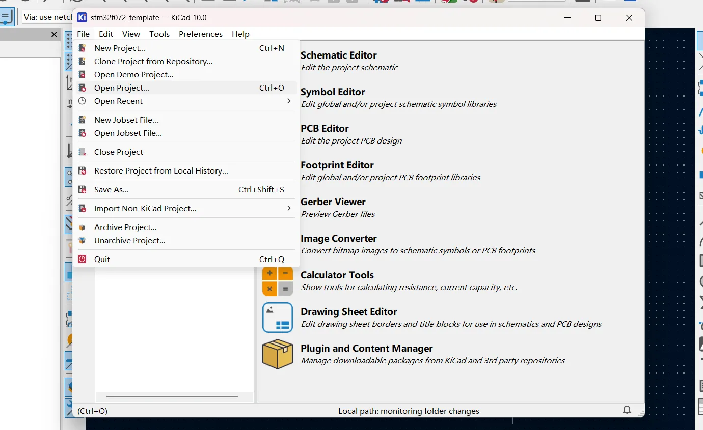
Native KiCad projects open directly. Use File → Open Project and select the .kicad_pro file. All associated schematic sheets, the board file, and project-specific libraries load together. This is the simplest and most reliable path.
Eagle Design Import
KiCad has mature support for Eagle XML-format projects (version 6 and later). Use File → Import → Non-KiCad Project and choose the Eagle option. Point KiCad at the folder containing the .sch and .brd files. The importer creates a new KiCad project with schematic and board data. Most connectivity, placement, and basic routing transfer successfully. Expect some footprint and library cleanup afterward.
DXF File Import
DXF files are commonly used for board outlines or mechanical keep-out regions. In the PCB Editor, use File → Import → Graphics (or the dedicated DXF import option). Select the DXF, choose the target layer (usually Edge.Cuts), and set the scale and units carefully. Always verify the imported outline is a closed shape before routing.
Legacy Project Migration
Older KiCad projects (version 5 and earlier) open in current versions with automatic conversion. After opening, save the project in the new format. Review library tables, because library paths and names changed significantly between major releases. Run ERC and DRC after migration to catch any residual issues.
Exporting Designs from KiCad
Gerber Export
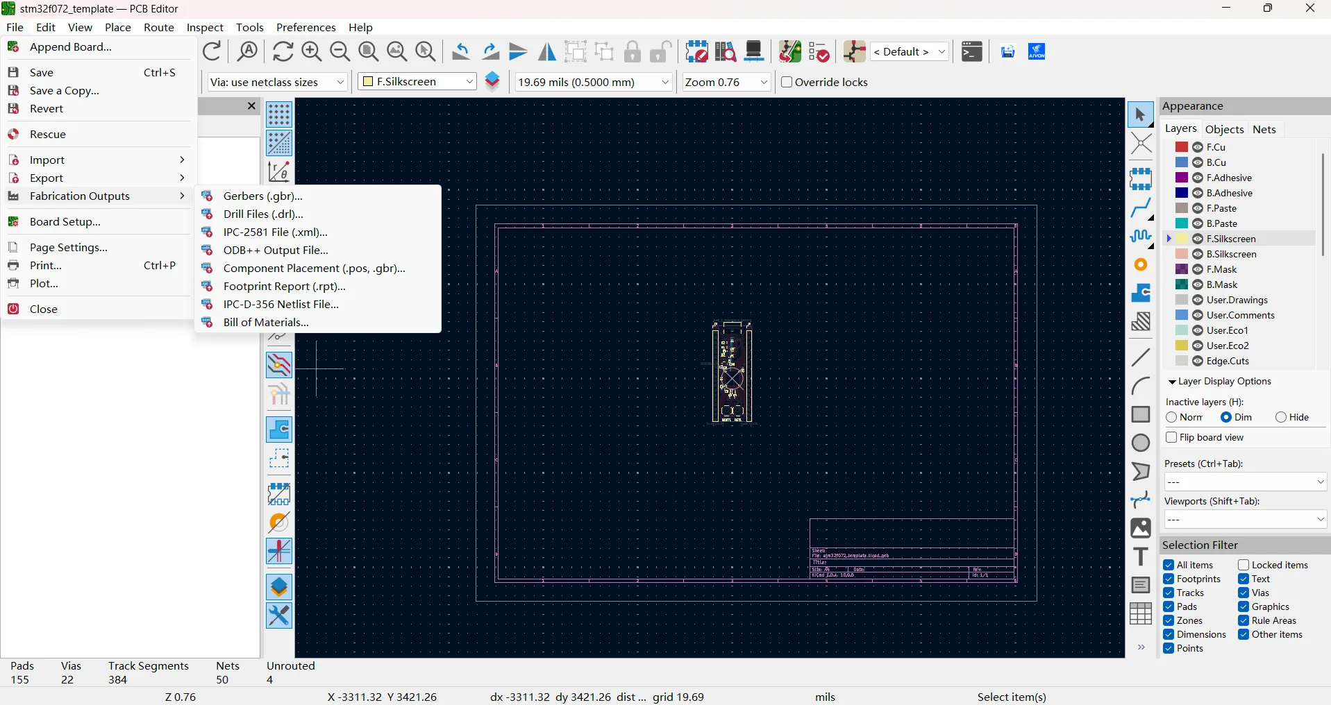
In the PCB Editor choose File → Fabrication Outputs → Gerbers (or the Plot icon). Select all required copper, soldermask, silkscreen, paste, and Edge.Cuts layers. Recommended practice includes:
- Using Protel-style filename extensions for broad fabricator compatibility
- Enabling "Subtract soldermask from silkscreen"
- Checking zone fills before plotting
- Choosing a dedicated output folder
Generate the files and immediately open them in GerbView for visual verification.
Drill File Generation
From the same Plot dialog (or Fabrication Outputs → Drill Files) produce Excellon drill files. Prefer millimetres and a single file containing both plated and non-plated holes unless the manufacturer requests separation. Include a drill map for easy checking.
STEP Model Export
File → Export → STEP produces a 3D model of the board and components for mechanical CAD. Enable "Substitute similarly named models" so VRML references are replaced by corresponding STEP models when available. Export board outline and components; tracks and zones are optional and increase file size.
Manufacturing Documentation Export
Additional outputs include:
- Bill of Materials (CSV or spreadsheet) from the schematic
- Pick-and-place (centroid) file from the PCB Editor
- PDF schematic and assembly drawings
- Position files for automated assembly
Collect these files into a single manufacturing package together with a short README describing layer stack-up and any special requirements.
Migrating from Other PCB Software
Altium to KiCad Workflow
KiCad (version 8 and later) includes a native Altium importer that handles .PcbDoc, .SchDoc, and library files. Use File → Import → Non-KiCad Project and select the Altium project. Copper geometry, nets, component placement, and many design rules transfer. After import:
- Re-link or recreate 3D models
- Review and re-enter high-speed or complex design rules
- Run full ERC and DRC
- Check library associations for missing footprints
Eagle to KiCad Workflow
The Eagle importer is one of the most mature. Import the project, then systematically replace or repair footprints that did not map cleanly. Rebuild any custom design rules and verify hierarchical sheets if the original design used them. Because Eagle free tiers imposed size and layer limits, many migrated designs gain new capability immediately in KiCad.
EasyEDA to KiCad Workflow
Export the EasyEDA design as a JSON or ZIP backup, then import via File → Import → Non-KiCad Project. Schematic and board data transfer, but library quality varies. Expect to re-assign or recreate footprints and to rebuild any specific part associations that do not exist in standard KiCad libraries.
In all migration cases, treat the first successful import as a starting point rather than a finished design. Plan time for cleanup, library work, and verification before considering the project production-ready.
Common Import and Export Problems
Missing Footprints
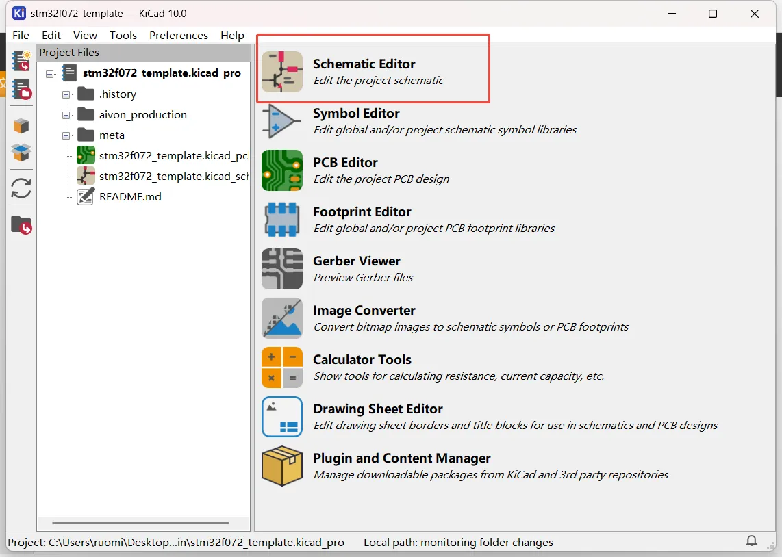
After import, many components show as missing footprints. This occurs because the original tool's library paths or naming conventions do not match KiCad. Solution: open the Schematic Editor, run the footprint assignment tool, and map each missing item to a KiCad footprint or a newly created one. Save the associations so future updates remain consistent.
Library Conflicts
Global and project library tables can conflict after migration. Prefer project-specific libraries for imported designs so the project remains self-contained. Avoid mixing old and new library table formats; reset to defaults if the project shows repeated library errors.
Layer Mapping Issues
Custom or non-standard layers in the source tool often map incorrectly or are ignored. During board import, review the layer-mapping dialog carefully. After import, inspect every technical layer (silkscreen, mask, paste, mechanical) and move graphics to the correct KiCad layers. Edge.Cuts must form a single closed outline.
Additional frequent issues include incomplete design-rule transfer, missing 3D models, and net-name differences that break cross-probing. Running ERC immediately after schematic import and DRC after board import surfaces most problems early.
A disciplined post-import checklist—library audit, layer inspection, full ERC/DRC, 3D review, and test manufacturing export—turns an imperfect conversion into a reliable KiCad project.
Import and export are not merely file conversions; they are the bridges that keep design intent intact across tools and into manufacturing. Mastering KiCad's native importers, careful layer and library handling, and precise manufacturing export settings reduces rework and ensures the boards that return from the fabricator match the design you approved.
FAQ
Q1: Can KiCad open Altium and Eagle projects directly?
A1: Yes. Use File → Import → Non-KiCad Project. Altium support improved significantly from KiCad 8 onward; Eagle XML projects have long been well supported. Expect some post-import cleanup of footprints and rules.
Q2: What files should I generate for PCB manufacturing?
A2: Gerber files for all required layers, Excellon drill files, a BOM, and a pick-and-place file if assembly is needed. Always verify the Gerbers in GerbView before sending.
Q3: Why do footprints disappear after importing a design?
A3: The original libraries are not present or use different names. Re-assign footprints in the Schematic Editor and save the associations. Creating project-specific libraries helps keep the design portable.
Q4: How do I import a board outline from a mechanical DXF?
A4: In the PCB Editor use File → Import → Graphics, select the DXF, set the correct units and scale, and place it on the Edge.Cuts layer. Confirm the outline is closed.
Q5: What is the most common cause of manufacturing-file problems?
A5: Incorrect layer selection or outdated zone fills during Gerber export. Always check zone fills before plotting, select every required layer, and inspect the output in GerbView.